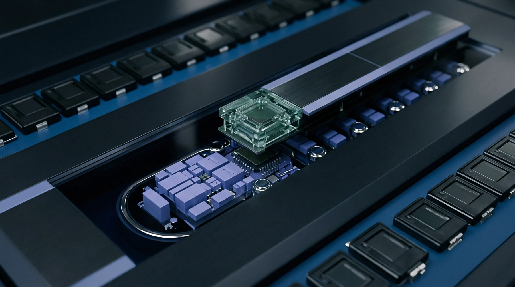
Calculating Worst Case Thermal Expansion Tolerances in Surface Mount Land Patterns
Worst case thermal expansion tolerances require arithmetic summation of material displacement and manufacturing variances to preserve solder fillet geometry.
Worst case thermal expansion tolerances require arithmetic summation of material displacement and manufacturing variances to preserve solder fillet geometry.

Fine pitch SMD land pattern design balances mechanical tolerances, stencil release physics, and routing strategies to maximize high-density assembly yield.

Extracting temperature-dependent interfacial fracture toughness along etched copper prevents reflow delamination and eliminates costly acoustic scan yield loss.
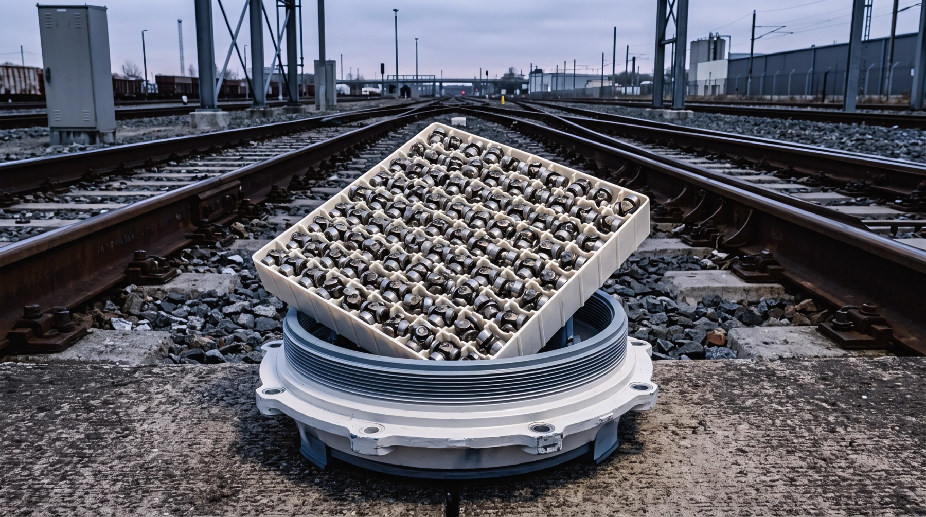
Extended baking at 125C drives solid-state intermetallic growth that depletes free tin, requiring verified nickel barriers to preserve terminal solderability.
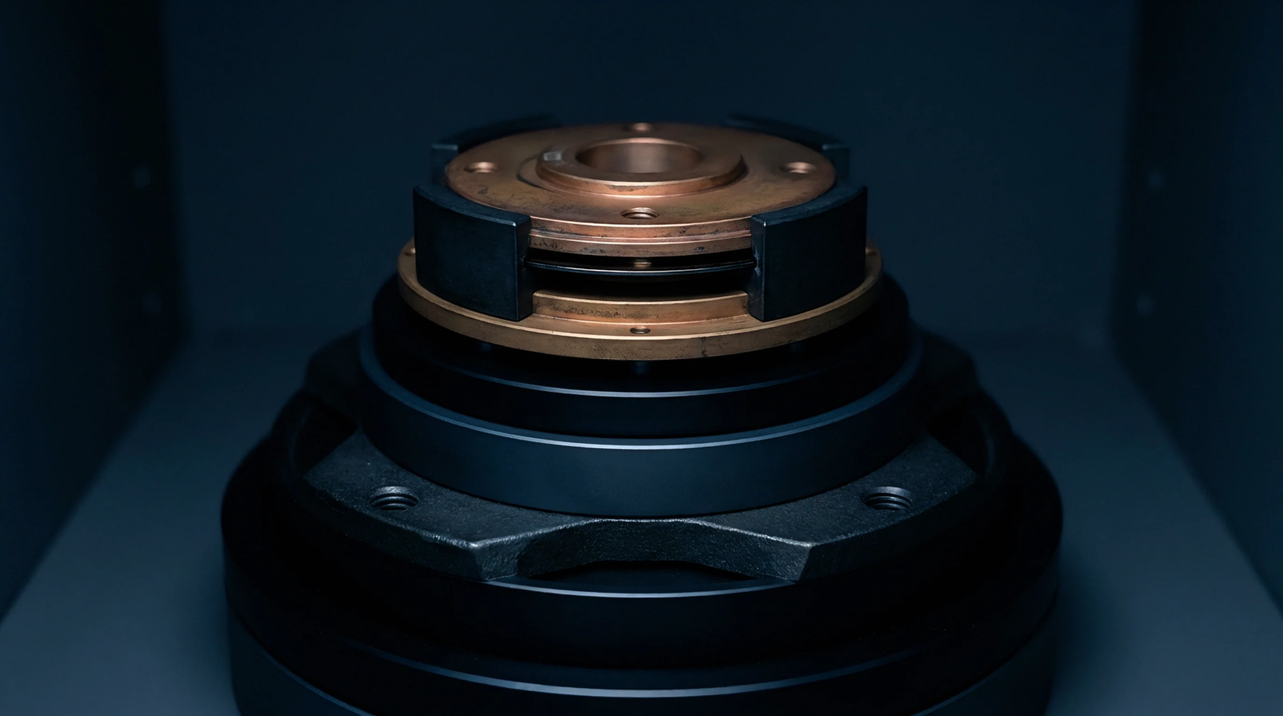
Coupled hygrothermomechanical finite element reflow modeling resolves moisture diffusion, steam pressure, and thermal expansion to prevent package delamination.
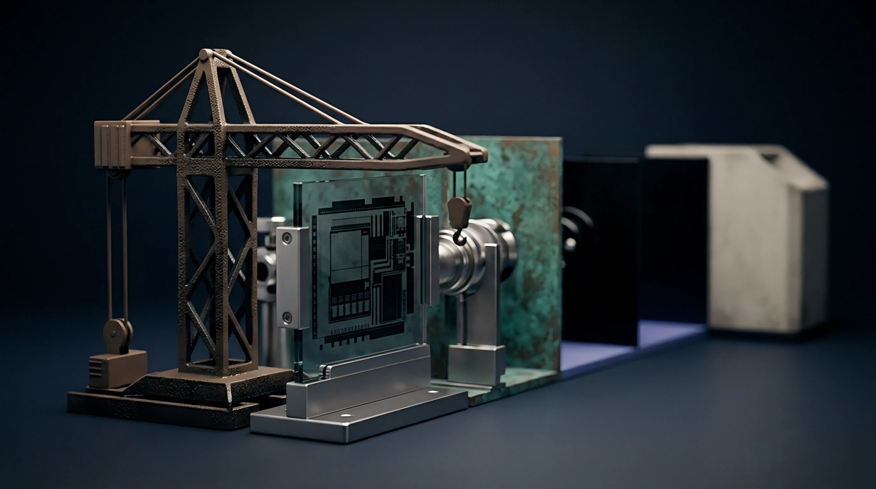
Fickian diffusion in thin encapsulants drives rapid moisture saturation, creating high internal steam pressures that trigger reflow delamination.

Calculating desorption kinetics and activation energy via multi-ramp thermal testing determines safe reflow limits and prevents package popcorning.

MSL classification dictates component allowable atmospheric exposure prior to reflow to prevent catastrophic internal delamination and joint failure.
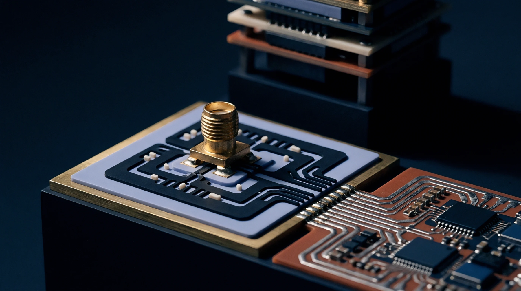
Determining clock low bounds across thermal cycles requires evaluating internal oscillator drift, package piezoresistive strain, and supply rail variations.

Host real time delays under clock stretching equal hardware SCL holding duration plus thread context switch and interrupt service routine preemption latency
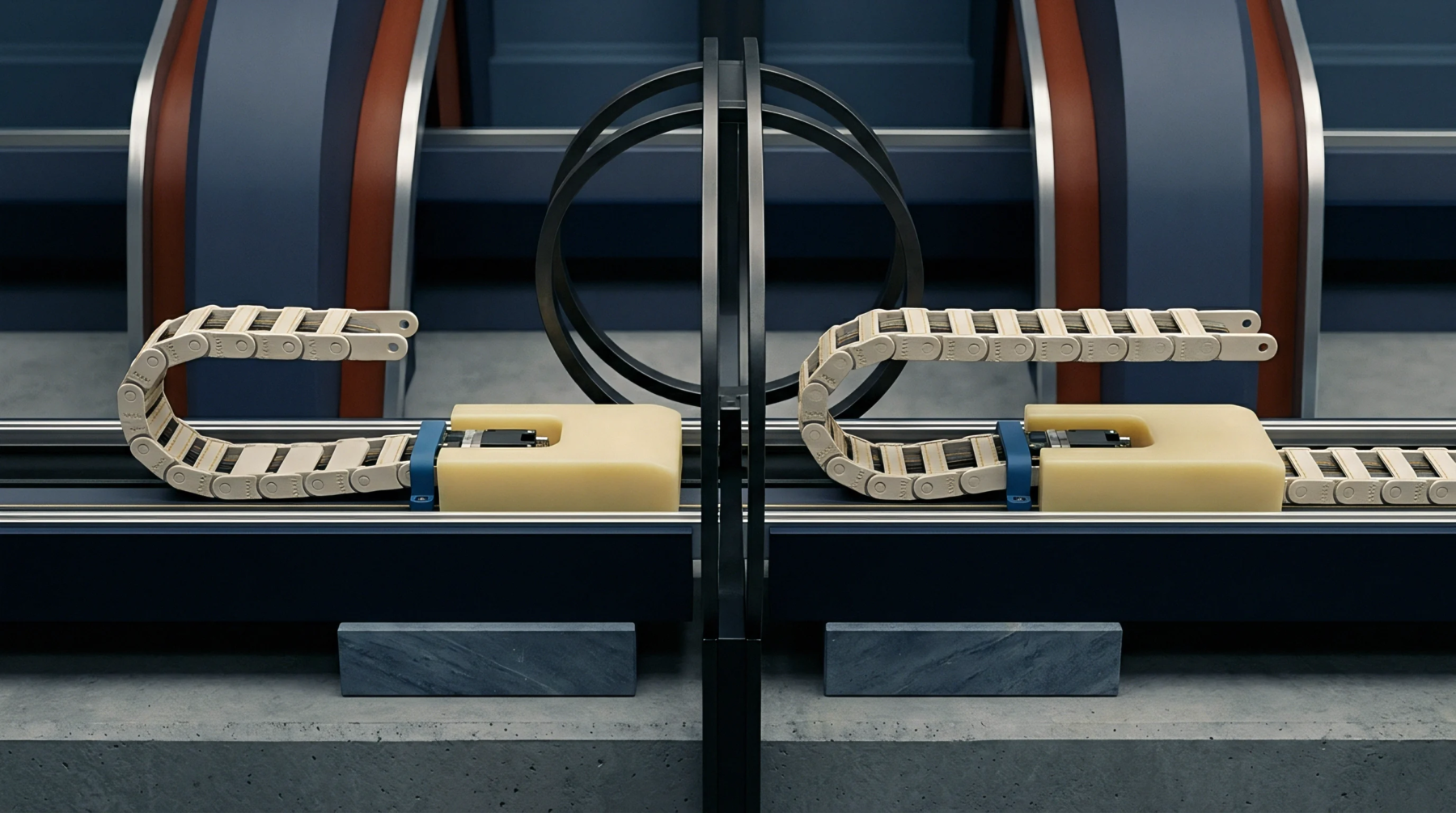
Clear stuck open-drain lines using nine manual clock cycles, followed by power-rail cutoff via load switch when latchup bypasses clock release.
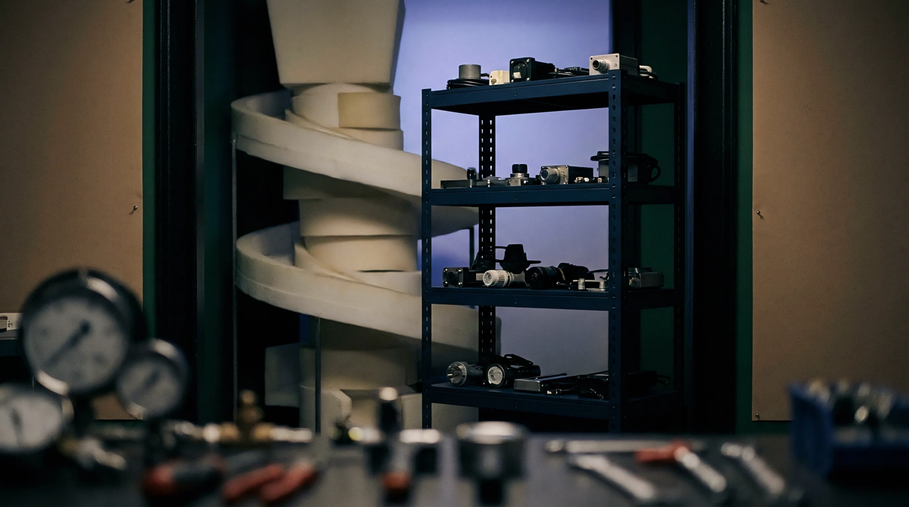
Factory-calibrated modules eliminate board-level thermal stress drift through mechanical decoupling and pre-programmed trim, justifying higher unit costs.

Modular serial sensors reduce firmware weeks and calibration expense at low volume, while discrete silicon preserves board area and unit margin past 6,500 units.

Discrete surface mount sensors minimize unit costs at high volume but demand board space, assembly controls, and firmware bring-up that modules eliminate.

Unannounced silicon steppings alter register maps and bus timing within catalog limits, driving massive firmware rework unless gated by contract terms.

Firmware abstraction layers add significant processor cycle overhead that inflates wake times and forces expensive microcontroller hardware upgrades.
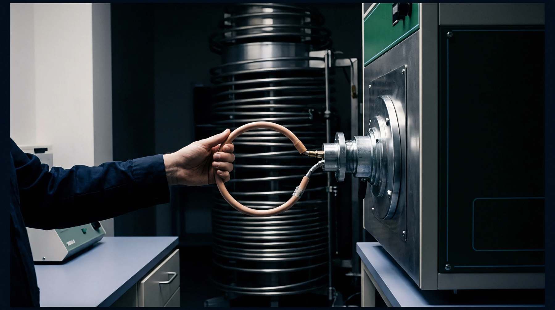
Selecting sensor packages and digital interfaces balances bus trace capacitance, pull-up current, thermal assembly stress, and firmware driver maintenance costs.
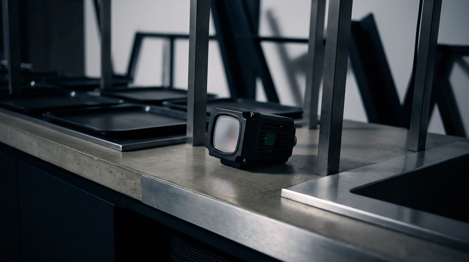
Thermal dissipation cycles induce package strain that skews bandgap reference outputs, necessitating symmetrical copper relief and strain-matched packaging.

Thermally isolates precision references from high-current output stages using symmetrical isometric layout, separate Kelvin return paths, and stress slots.
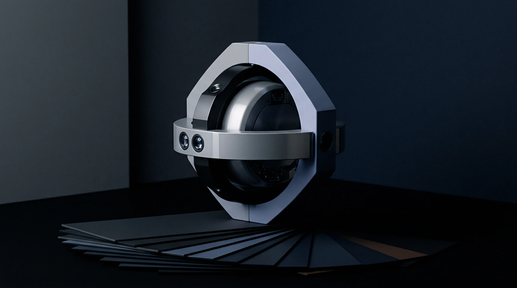
Mitigate reference thermal drift by isolating footprints with milled PCB slots, enforcing post-reflow stabilization bake, and selecting ceramic packaging.
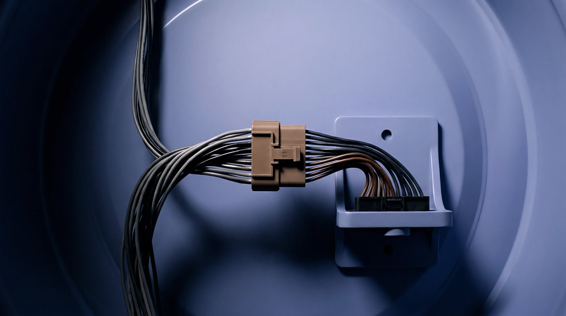
Accumulated line capacitance degrades open-drain rise times, demanding active acceleration or branch buffering to maintain deterministic software enumeration.

Cascade enable logic eliminates individual chip-select routing across dense sensor arrays by propagating a single hardware token down a shared serial bus.
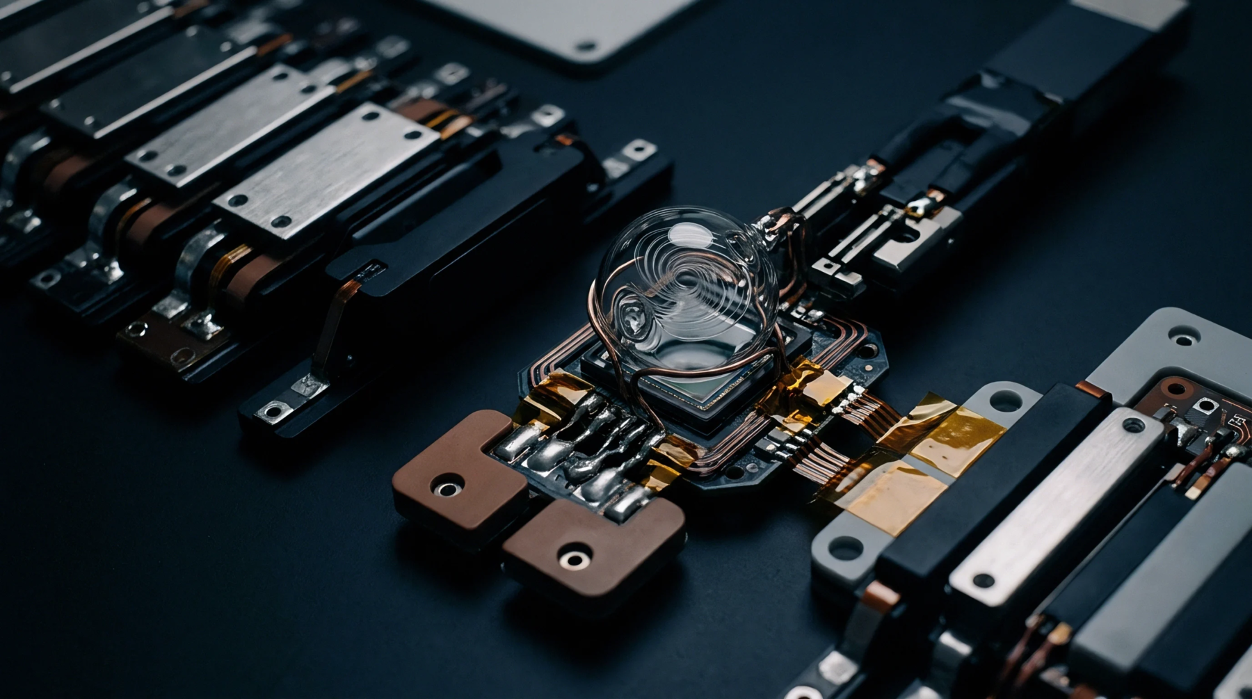
Dynamic address assignment eliminates external multiplexers in dense sensor arrays, trading minor firmware development time for reduced PCB routing and lower bill-of-materials costs.

Active dynamic translation uses pulsed current injection to overcome high multi-drop bus capacitance, maintaining rise times without exceeding sink currents.

Hardware address translators eliminate driver overhead and preserve trunk routing, while bus multiplexers isolate bus capacitance and cut bill of materials costs.

Manage identical I2C devices by combining hardware pin strapping, pass-gate multiplexers, or inline address translators to isolate matching identifiers.

Polyurethane and epoxy viscoelastic stress relaxation causes time-dependent zero offset drift in encapsulated piezoresistive sensors inside stainless housings.
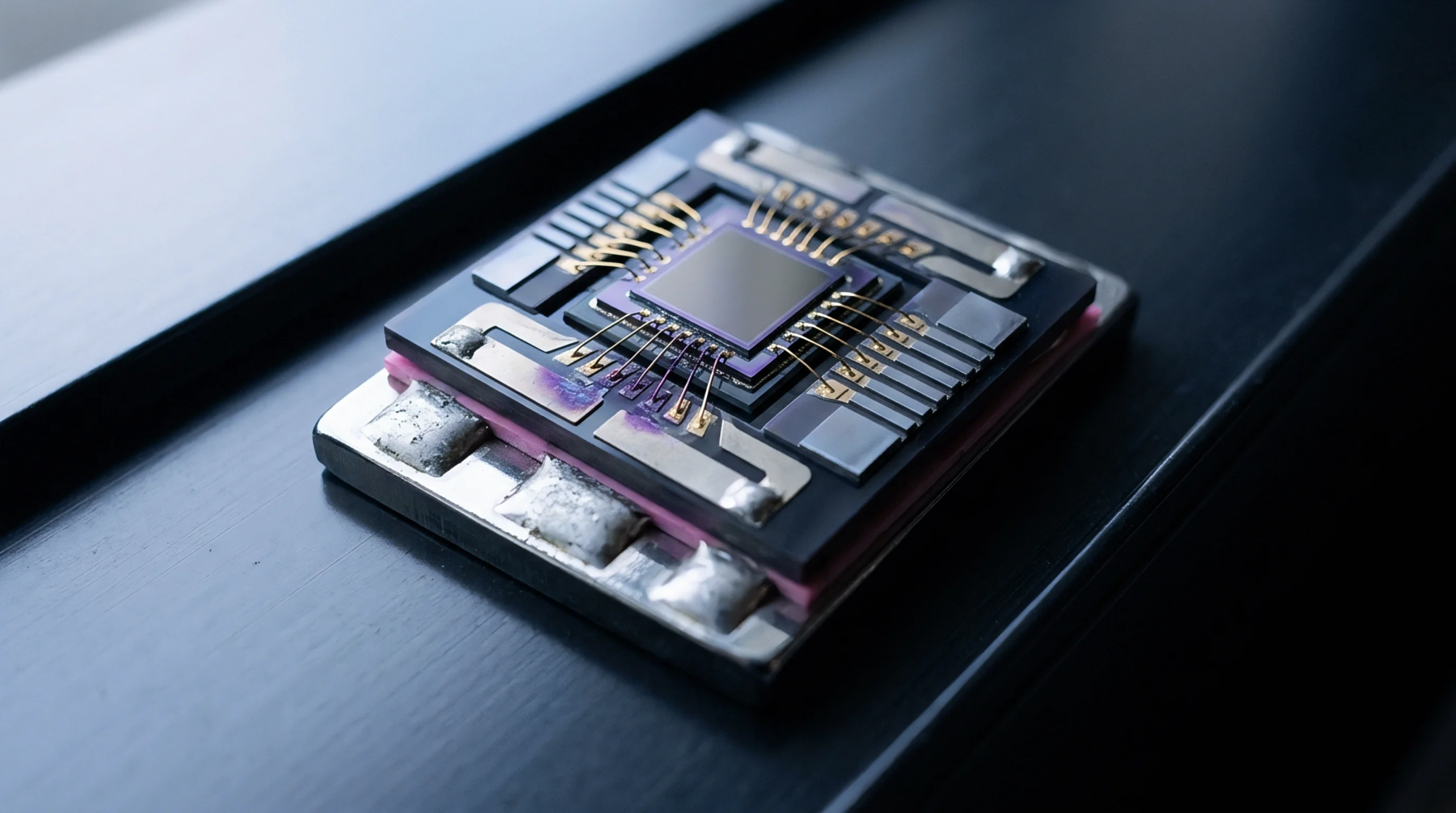
Zero offset drift in potted piezoresistive sensors requires decoupling die stress via soft silicone gels before applying ASIC polynomial thermal compensation.

Compliant silicone buffer layers isolate piezoresistive silicon dies from rigid epoxy cure shrinkage, eliminating offset drift in harsh industrial sensors.

Board strain shifts uncompensated sensor zero points by millivolts, requiring isolation trenches or custom assembly when volumes surpass tooling payback.
Expertise is a utility, not a secret. sentiention™ publishes its working knowledge as open reference: intelligence layer covering the materials it sources, the markets it enters, and the reference that serves both.