
Thermal Relief Routing Rules to Stabilize Sensitive Analog References
Symmetrical thermal relief spokes and matched copper routing stabilize precision analog references by mitigating thermoelectric EMF and solder strain.
Symmetrical thermal relief spokes and matched copper routing stabilize precision analog references by mitigating thermoelectric EMF and solder strain.
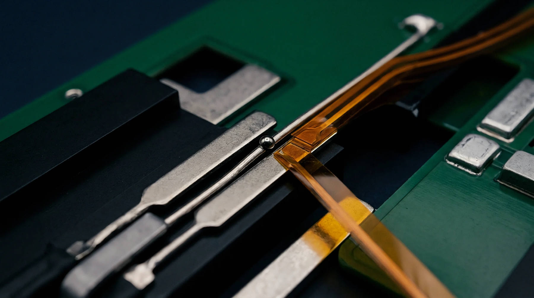
Precision voltage reference layout demands mechanical isolation slits, symmetric thermal copper paths, and compliant leads to eliminate piezoresistive drift.

Substrate moisture uptake increases trace capacitance and reduces microstrip impedance, requiring ground-shielded striplines or hydrophobic coatings.

NMOS pass gate level shifters cause VGS threshold drops that erode VIH logic margins, requiring active push-pull buffers or tuned bias voltage rails.

Dynamic bus capacitance equals host load plus off-state switch parasitics and active segment trace and pin loads across operational state combinations.
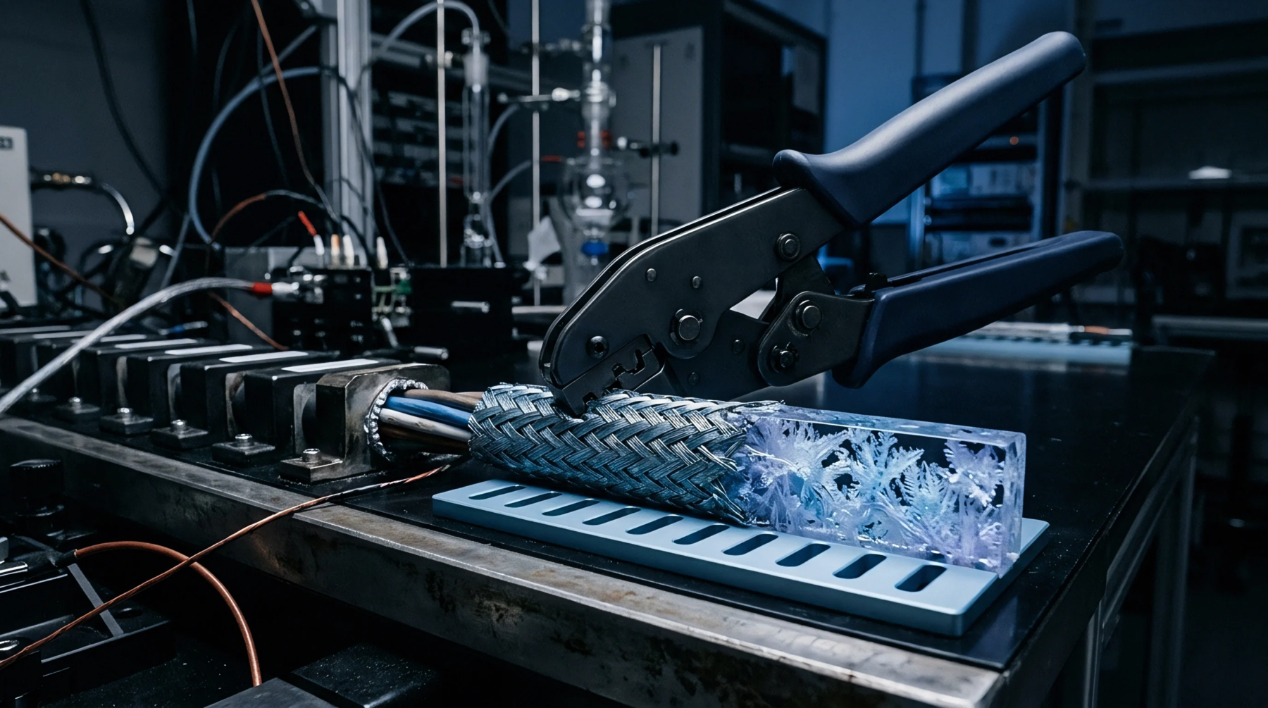
Cascade multi-tier buses by matching loaded line impedances and limiting physical stub lengths to under one-third of the signal edge transition length.
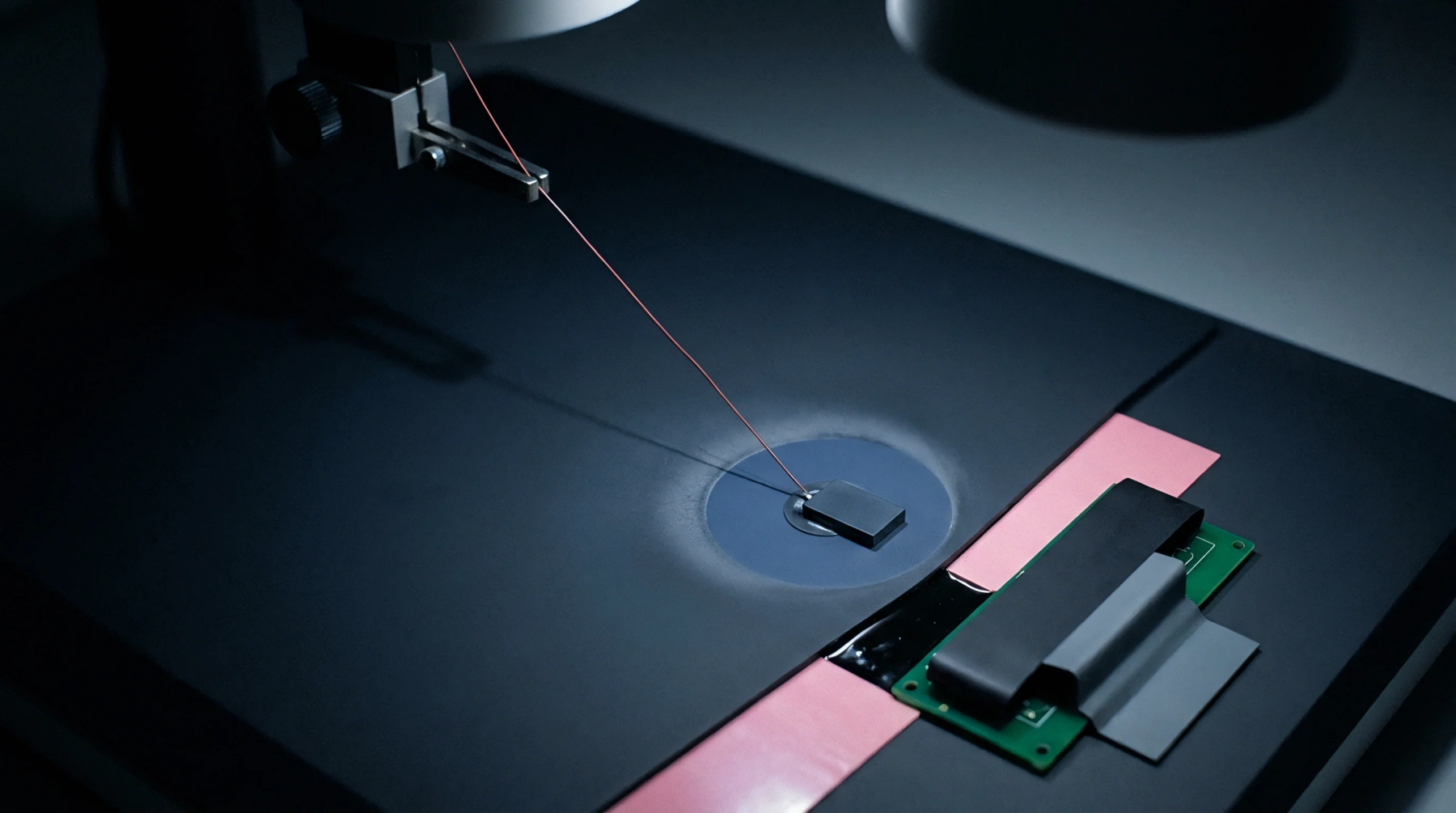
Cascaded multiplexer trees require parasitic capacitance checks per stage to keep total load below bus standard limits and prevent signal corruption.

Hardware I2C multiplexers isolate identical peripheral addresses and split capacitive loads across independent, switchable bus branches.

Dynamic sensor address resolution in high-noise arrays requires differential physical-layer isolation, sequential gate waking, and robust nine-clock recovery.

Active bus accelerators and differential transceivers preserve signal integrity across high-capacitance sensor lines by isolating slow capacitive RC edges.

Addressing multi-channel sensors on shared two-wire buses relies on address pin strapping, active bus switches, or in-line offset address translation ICs.
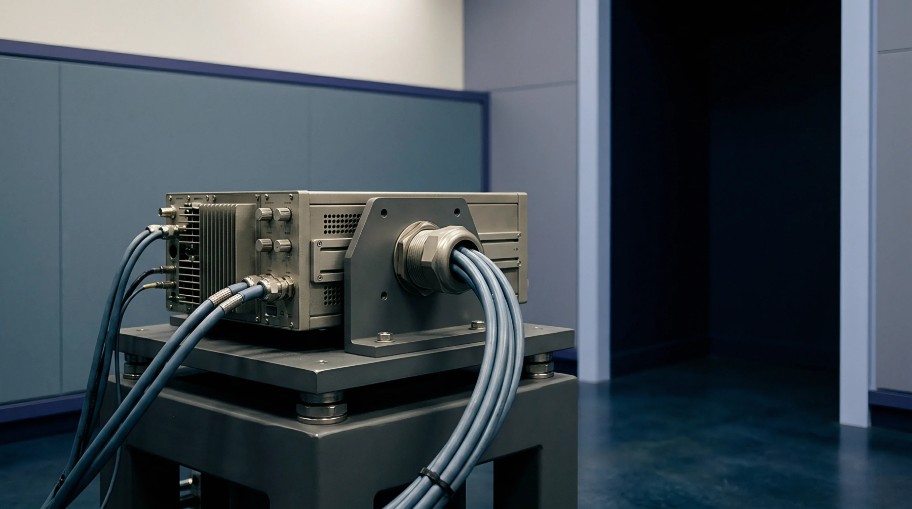
Dynamic shield braid fatigue converts common-mode engine noise into differential sensor error, favoring digital bus transceivers over heavy shielded cabling.

Common-mode harness termination requires matched magnetic series impedance, minimal pad ESL, and direct 360-degree chassis bonding at the connector boundary.
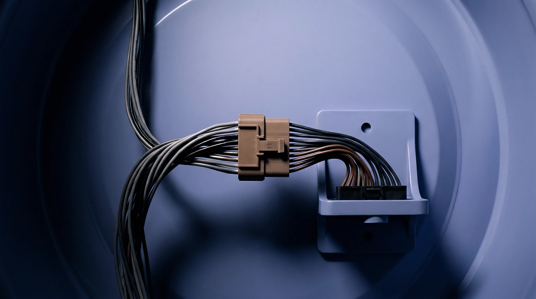
High-temperature differential pairs maintain 100-ohm impedance by matching thermal permittivity drift with trace spacing expansion tolerances across operating gradients.

Resolve bus accelerator offset mismatches by inserting series damping resistors at sensor drops and matching buffer static offsets to receiver low thresholds.

Tame accelerator switching spikes across remote sensor cabling by matching series damping resistors to line impedance and clamping ground bounce.

Active bus buffers conquer excessive capacitance by isolating bus segments or accelerating edges, demanding careful offset voltage matching below 2.5V.

Dielectric shrinkage and freeze-out change cable capacitance, rotating signal phase and skewing four-wire cryogenic sensor readings.

Shield topology selection governs high-frequency sensor signal distortion through optical coverage, geometric symmetry, and 360-degree termination mechanics.
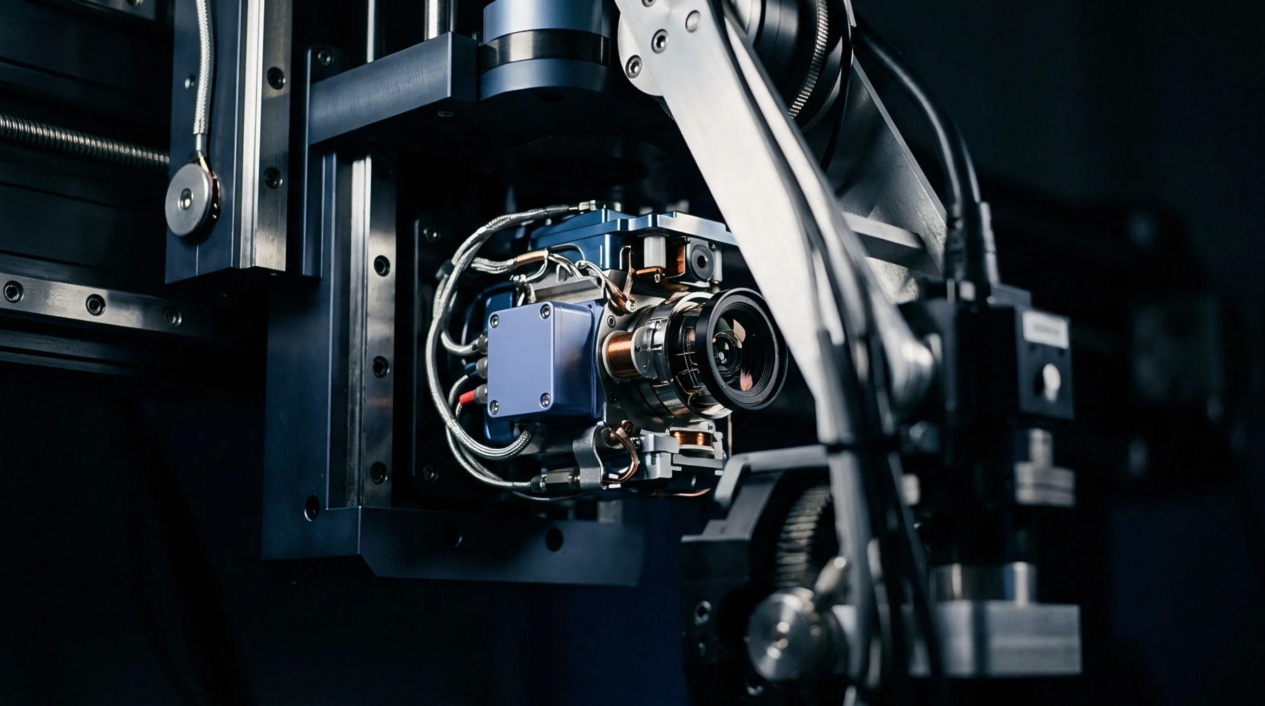
Estimate unshielded line-to-line capacitance from conductor radius, dielectric constant, and wall thickness using inverse hyperbolic cosine formulations.

Extract submodel cut boundary displacements from coarse PCB models to compute local inelastic strain energy density for accurate thermal shock life prediction.
Calibrated Anand viscoplastic modeling predicts solder joint thermal fatigue life by coupling rate-dependent strain energy accumulation to board-level packaging geometry.

Wafer-level package shear mechanics rely on ball standoff height, pad geometry, and underfill to mitigate thermal expansion mismatch across solder joints.

Resin squeeze in dense multilayer stackups compresses dielectric thickness by up to 15 percent, shifting differential impedance downward by over 10 ohms.
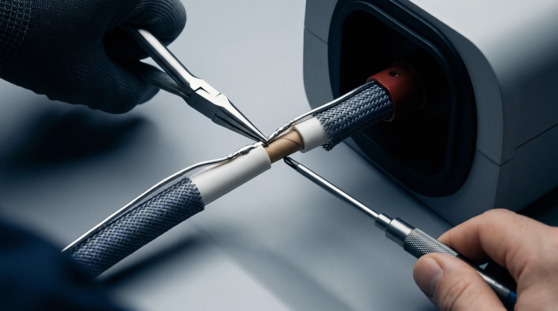
Microvia pad planarization eliminates solder joint voids and stabilizes high-frequency trace impedance by controlling dimple depth and copper cap topography.

Area ratios above 0.66 secure repeatable solder paste release on fine-pitch arrays, while specialized foil coatings permit acceptable transfer down to 0.50.

Thermal cycling creates mold compound delamination voids that ionize under electric fields, causing partial discharge failures exceeding five picocoulombs.
Select compact isolated signal packages by matching CTI ratings to creepage rules and holding parasitic capacitance under 1 pF to survive 100 kV/µs transients.

Select surface mount isolation packages by matching CTI material groups and working voltages to mandatory creepage and clearance distances under IEC 60664-1.

Dynamic package shear stress produces non-inverting thermal hysteresis loops that defeat memoryless polynomial matrix compensation in multi-axis sensors.
Expertise is a utility, not a secret. sentiention™ publishes its working knowledge as open reference: intelligence layer covering the materials it sources, the markets it enters, and the reference that serves both.