
Determining Break Even Volume Boundaries for Custom Sensor PCB Integration
Discrete sensor chip-down integration breaks even above fifteen thousand units where bill-of-materials savings overcome tooling and test fixture outlays.
Discrete sensor chip-down integration breaks even above fifteen thousand units where bill-of-materials savings overcome tooling and test fixture outlays.

Multi-channel sensor integration on standard two-wire buses demands balancing parasitic bus capacitance, address resolution, layout geometry, and landed unit cost.

Dynamic thermal gradients induce structural strain and bias errors that static calibrations miss, requiring real-time state observer algorithms.
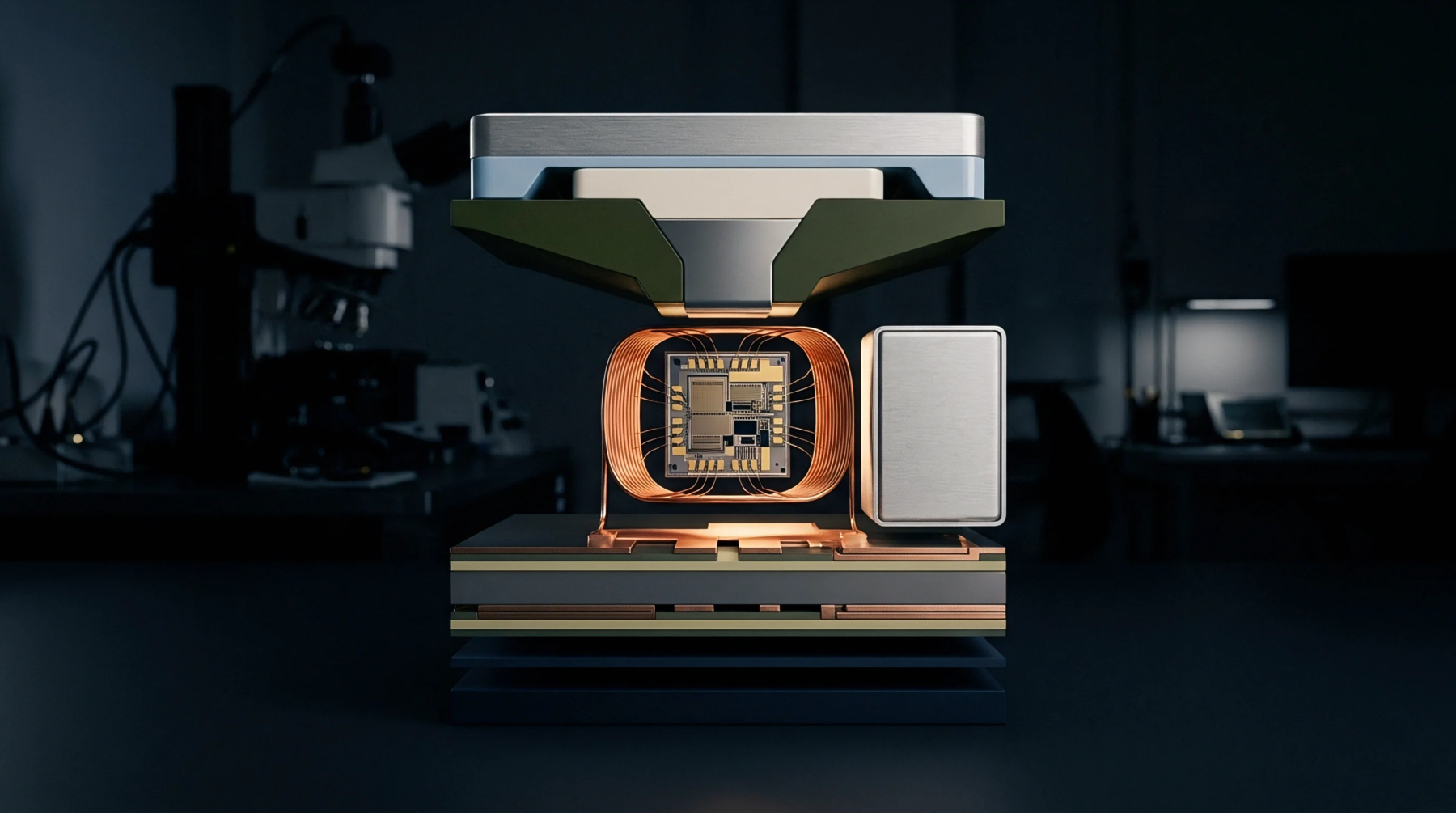
Matching package creepage distance to board pollution degree prevents arc flash failure while maintaining high density surface mount assembly yields.

Component obsolescence decisions require balancing upfront board redesign NRE against multi-year nitrogen storage capital tie-up and solderability decay risks.

Wafer bank conversion agreements convert raw iso-die into multi-form sensor packages, shifting supply risk while managing lead time, yield, and bus drift.

Discrete SMD sensors break even over integrated serial modules above fifty thousand units when assembly yields exceed ninety nine percent.

Dynamic address assignment eliminates multiplexers in dense sensor arrays through cascade enable lines or software ARP, reducing PCB area while raising firmware bring-up requirements.
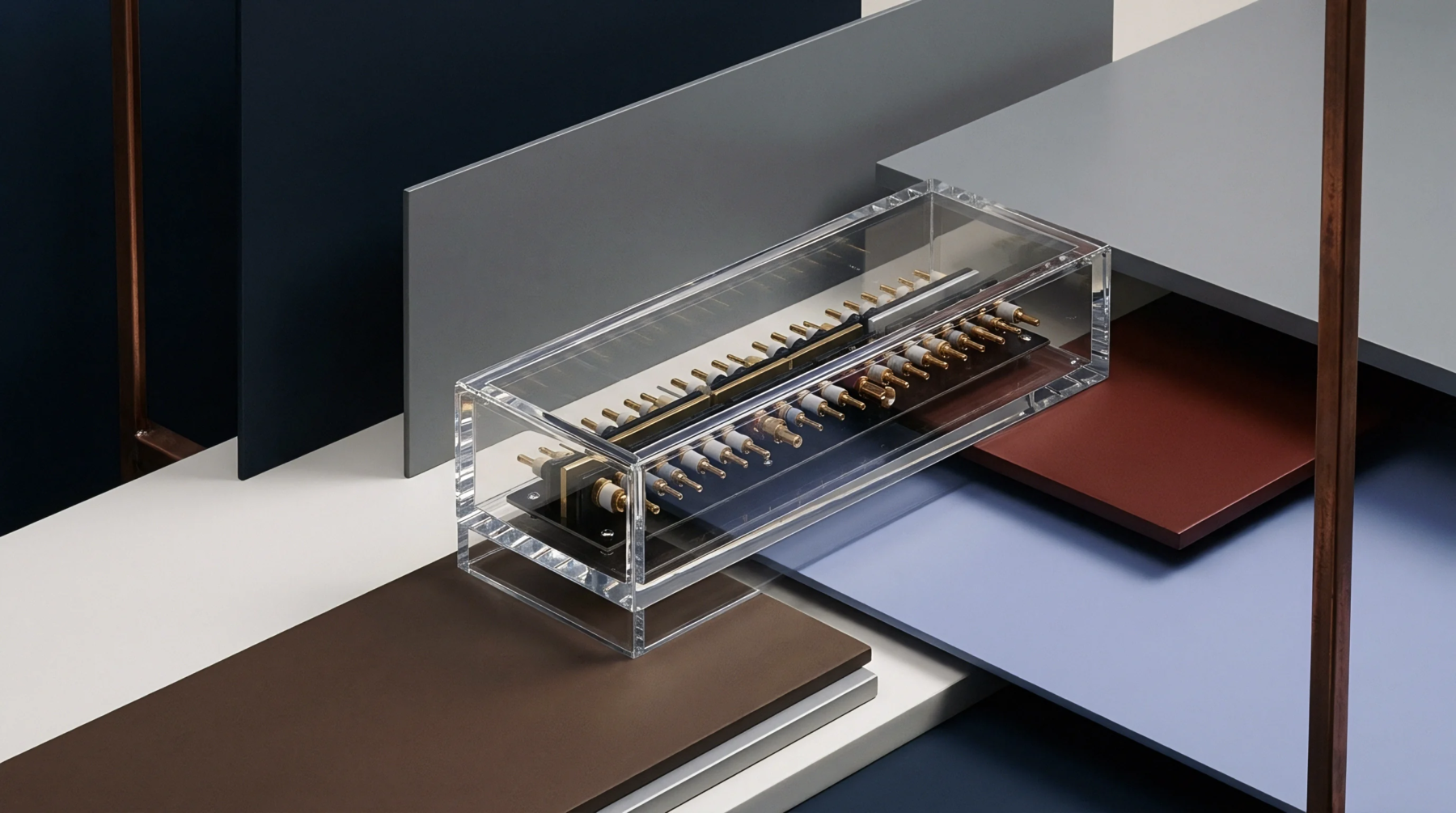
Sourcing sensor modules eliminates 4 to 12 weeks of driver engineering, flipping break-even economics below 15,000 units despite higher unit BOM prices.
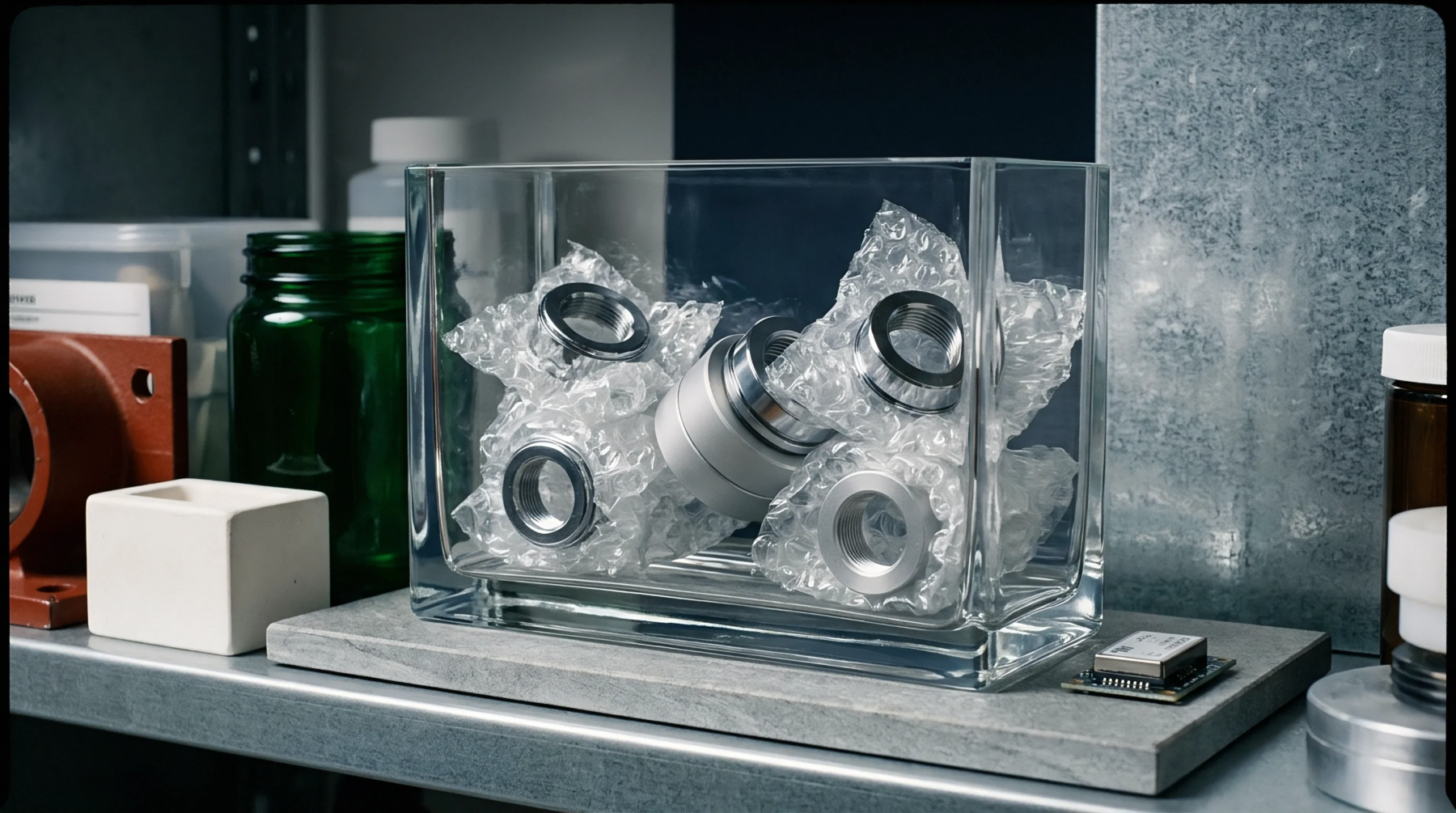
Substituting high-grade physical sensors with multi-element algorithms saves unit cost but adds firmware overhead, thermal drift risks, and qualification expenses.
Expertise is a utility, not a secret. sentiention™ publishes its working knowledge as open reference: intelligence layer covering the materials it sources, the markets it enters, and the reference that serves both.