
Designing Cascaded I2C Multiplexer Topologies for High Density Hardware
Cascaded I2C multiplexers resolve address collisions in high-density systems by isolating bus segments, requiring strict RC capacitance and switch resistance control.
Cascaded I2C multiplexers resolve address collisions in high-density systems by isolating bus segments, requiring strict RC capacitance and switch resistance control.

Multi-channel sensor integration on standard two-wire buses demands balancing parasitic bus capacitance, address resolution, layout geometry, and landed unit cost.

Suppress high frequency parasitic coupling under thermal stress by using quad-twisted high-temp fluoropolymer cable with 360-degree shield crimps and CMC filtering.

Active pull-up buffers restore slew rates on high-capacitance sensor lines without raising low-level output voltages or violating static sink limits.

Twisted pair cabling shunt capacitance equals mutual line capacitance plus half the line-to-shield capacitance, setting hard limits on sensor signal bandwidth.

Thermomechanical fatigue modeling for WLCSP solder arrays requires mapping viscoplastic Anand strain energy density to predict field thermal cycling failures.

Fine-pitch package assembly requires pairing stencil foil reductions with thin outer-layer dielectrics to maintain solder transfer and controlled impedance.

Matching package creepage distance to board pollution degree prevents arc flash failure while maintaining high density surface mount assembly yields.

Matrix compensation algorithms correct non-linear thermal piezoresistive drift by mapping raw bridge and temperature counts through fixed-point polynomial surfaces.
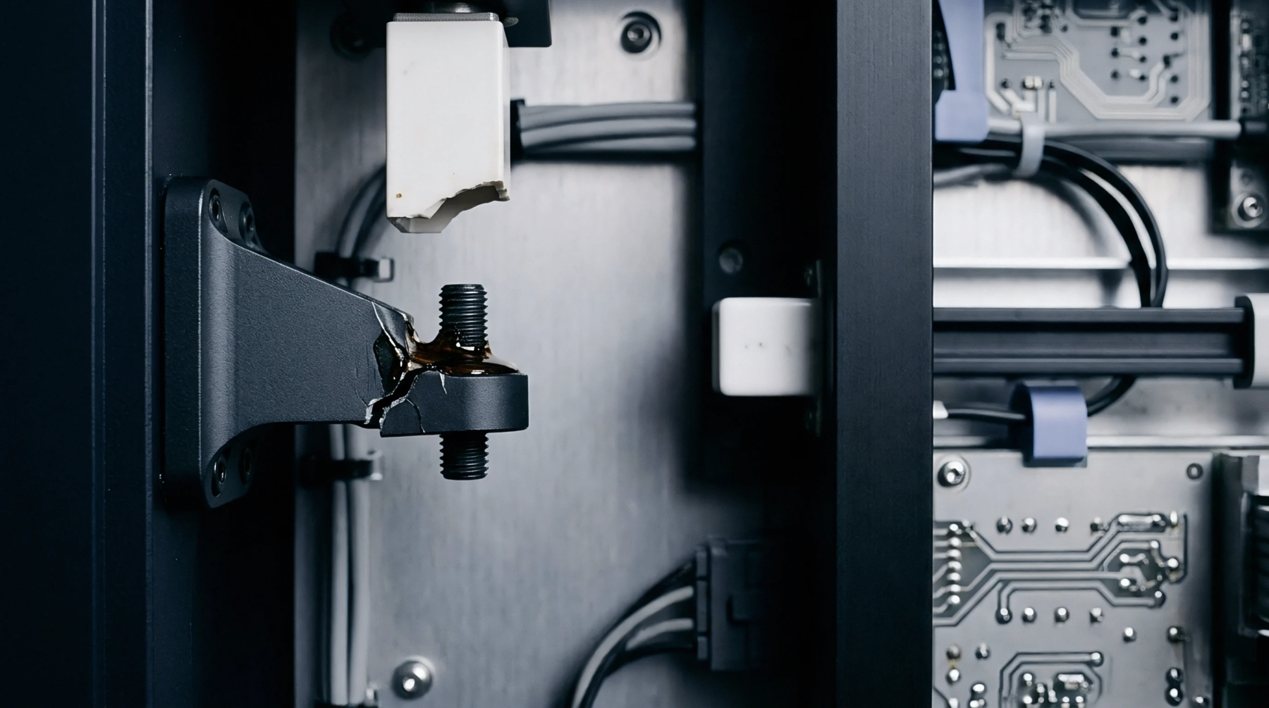
Precise Wheatstone bridge zero-point stability requires matching piezoresistive crystal orientation with thermo-mechanical strain isolation in the packaging stack.

Asymmetric thermal expansion shifts bandgap voltage via piezoresistive substrate stress; mechanical slots and ceramic packaging isolate critical reference nodes.

Dynamic PCB thermal gradients cause substrate flexing that alters converter resistor ladder ratios via piezoresistive strain, driving gain drift.

Board flexure stress couples to analog dies via solder joints and mold compounds, shifting bandgap voltages up to 10 millivolts under thermal cycling.
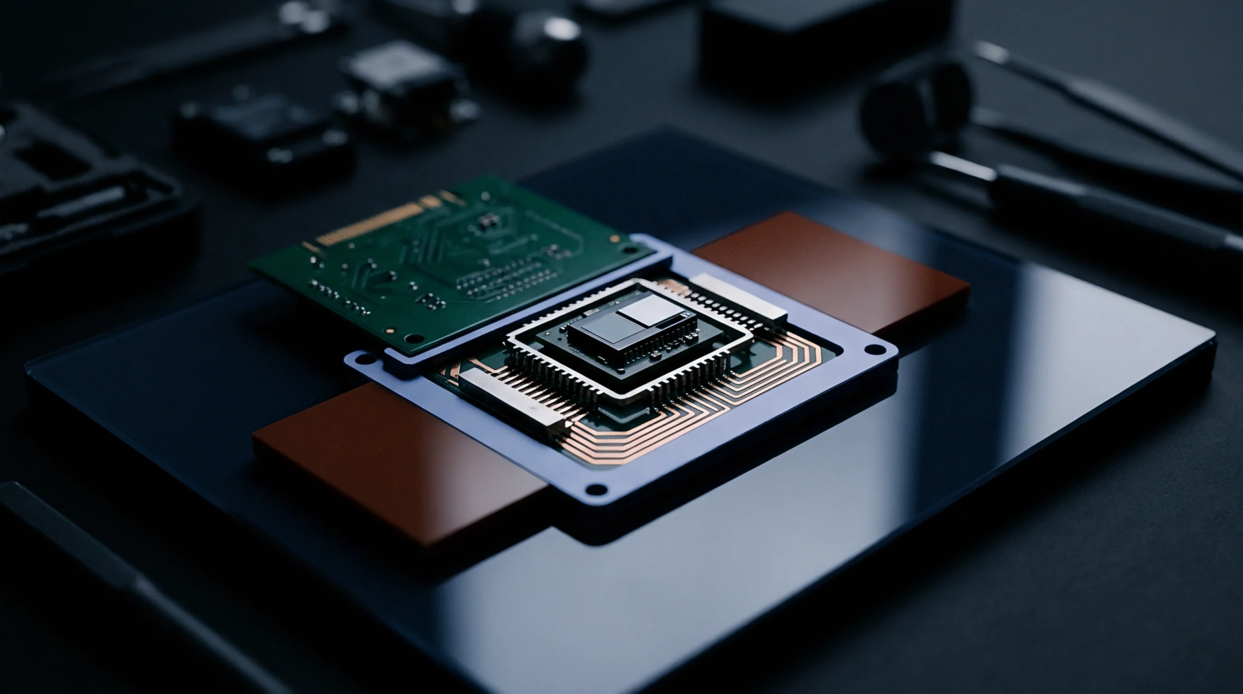
Common centroid transistor layouts for bandgap cores cancel linear thermal and lithographic gradients, reducing post-packaging output drift below 5 ppm per C.
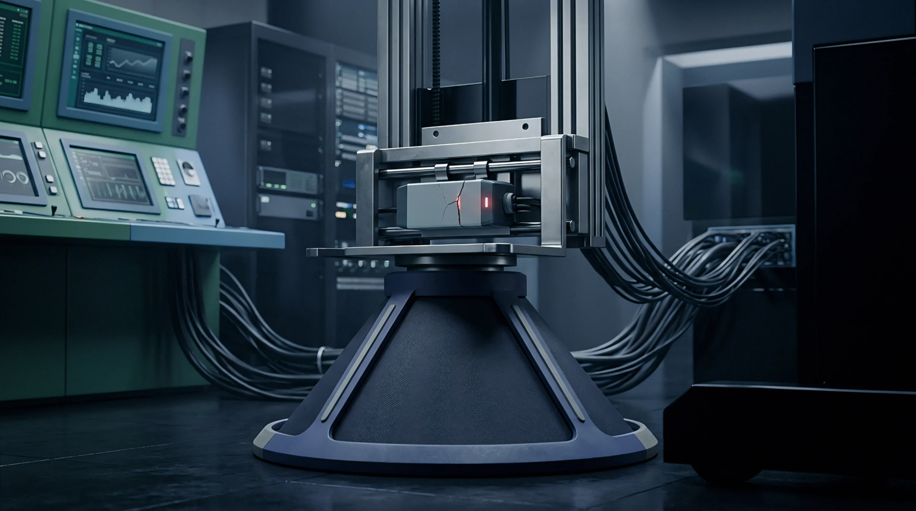
Dynamic asymmetric board strain couples into silicon piezoresistors via solder joints, causing uncompensated baseline drift mitigated by PCB isolation slots.

Asymmetric thermal gradients across precision references induce microvolt offsets through Seebeck potentials and piezo-resistive stress imbalance.

Monolithic reference thermal drift sensitivity combines silicon junction non-linearities, piezoresistive mechanical package stress, and solder reflow hysteresis.

Dual stage Langmuir kinetics dictate that bound moisture desorbs into steam during reflow, driving delamination and sensor offset drift unless bake profiles clear bound water.
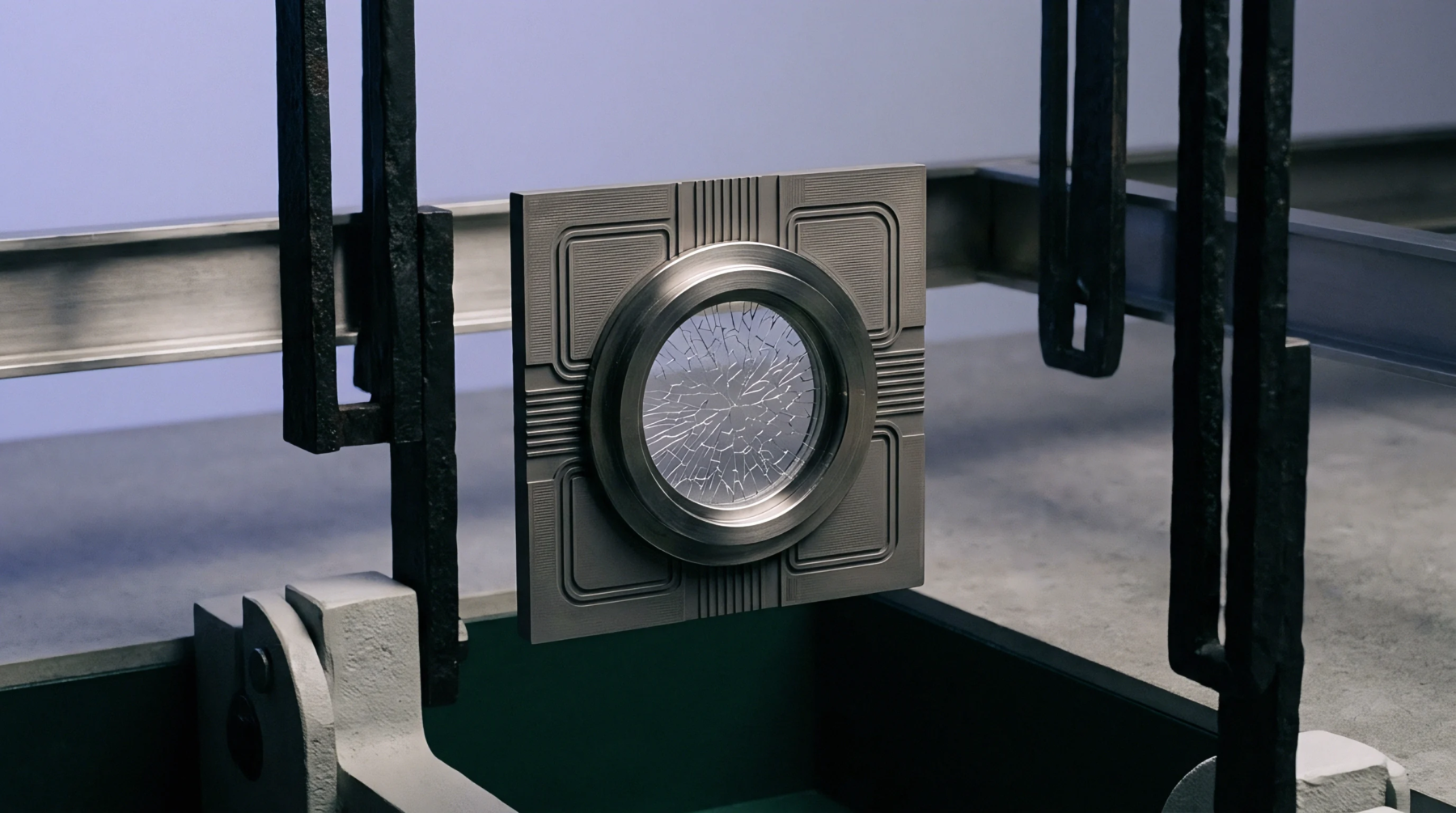
Interfacial hygroscopic swelling stress arises from differential moisture expansion, compounding thermal mismatch and driving package delamination during reflow.

Moisture kinetics in epoxy molding compounds dictate reflow vapor pressure, package strain, and MSL floor life across surface mount assembly lines.

Active buffers isolate bus capacitance beyond 400 picofarads by segmenting traces and using static voltage offsets or edge accelerators to meet timing limits.

Resolve multi-sensor address collisions using pin-strapped dividers, digital multiplexers, or active translators sized against bus capacitance and firmware costs.

Dynamic thermal cycling drives moisture pumping across organic probe seals, dropping surface insulation resistance and inducing analog bridge calibration drift.

Selecting surface mount sensor packages requires balancing land-pattern mechanical stress and reflow limits against bus integration effort and unit yield cost.

Component obsolescence decisions require balancing upfront board redesign NRE against multi-year nitrogen storage capital tie-up and solderability decay risks.

Structure IC orders using exact full-reel increments matching historical baseline entitlements to bypass automated shortage allocation cuts.

Enforceable sensor discontinuance contracts extend baseline JESD48B notice windows to twelve months LTB and cap buffer stock storage risks through strict MSL controls.

Automated wafer level probe fuse verification guarantees individual chiplet traceability across high density packaging reflow cycles before costly module assembly

Automated auditing of chiplet identification registers via IEEE 1838 interfaces prevents multi-die package misconfiguration before final encapsulation.

Verifying silicon die revision registers during boot ensures firmware compatibility and prevents unannounced stepping changes from causing field failures.
Expertise is a utility, not a secret. sentiention™ publishes its working knowledge as open reference: intelligence layer covering the materials it sources, the markets it enters, and the reference that serves both.