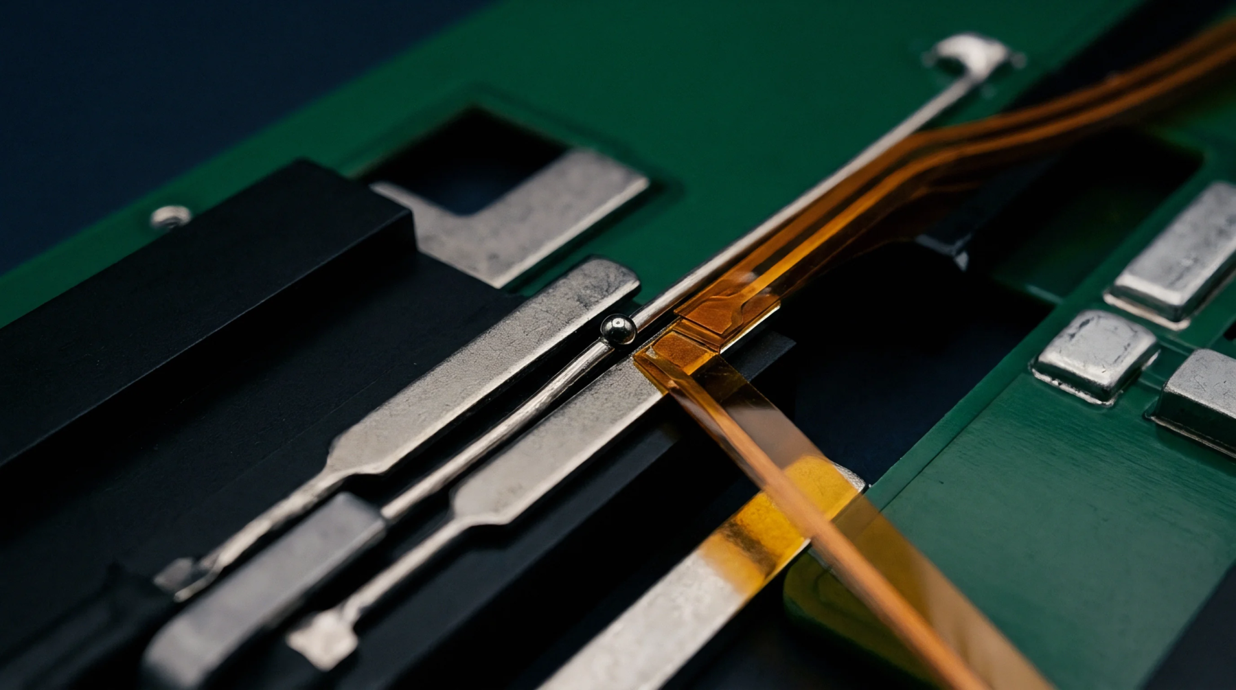
Minimizing Circuit Board Strain Propagation in Surface Mounted Pressure Sensors
Milled PCB isolation slots and controlled solder standoff heights decouple surface mount pressure sensors from assembly flexure and thermal board strain.
Milled PCB isolation slots and controlled solder standoff heights decouple surface mount pressure sensors from assembly flexure and thermal board strain.

Mitigate bandgap thermal stress errors using compliant leaded packages, PCB isolation slots, polyimide die buffers, and stabilized factory calibration.

Cross-quad common-centroid bandgap layouts cancel linear thermal gradients, while PCB isolation slots prevent package piezoresistive strain from shifting Vbe drift.

Mitigate surface-mount precision reference thermomechanical drift using three-sided PCB slot moats, compliant land patterns, or hermetic ceramic packages.
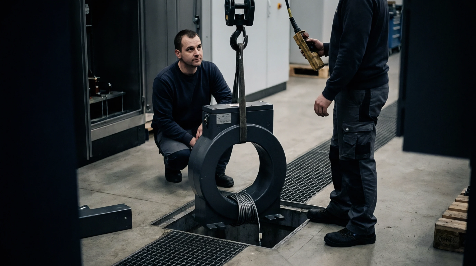
Precision voltage reference accuracy depends on isolating packages from board flexure, balancing trace Seebeck junctions, and blocking thermal conduction paths.

Cascaded I2C multiplexers resolve address collisions in high-density systems by isolating bus segments, requiring strict RC capacitance and switch resistance control.

Multi-channel sensor integration on standard two-wire buses demands balancing parasitic bus capacitance, address resolution, layout geometry, and landed unit cost.

Matrix compensation algorithms correct non-linear thermal piezoresistive drift by mapping raw bridge and temperature counts through fixed-point polynomial surfaces.

Asymmetric thermal expansion shifts bandgap voltage via piezoresistive substrate stress; mechanical slots and ceramic packaging isolate critical reference nodes.
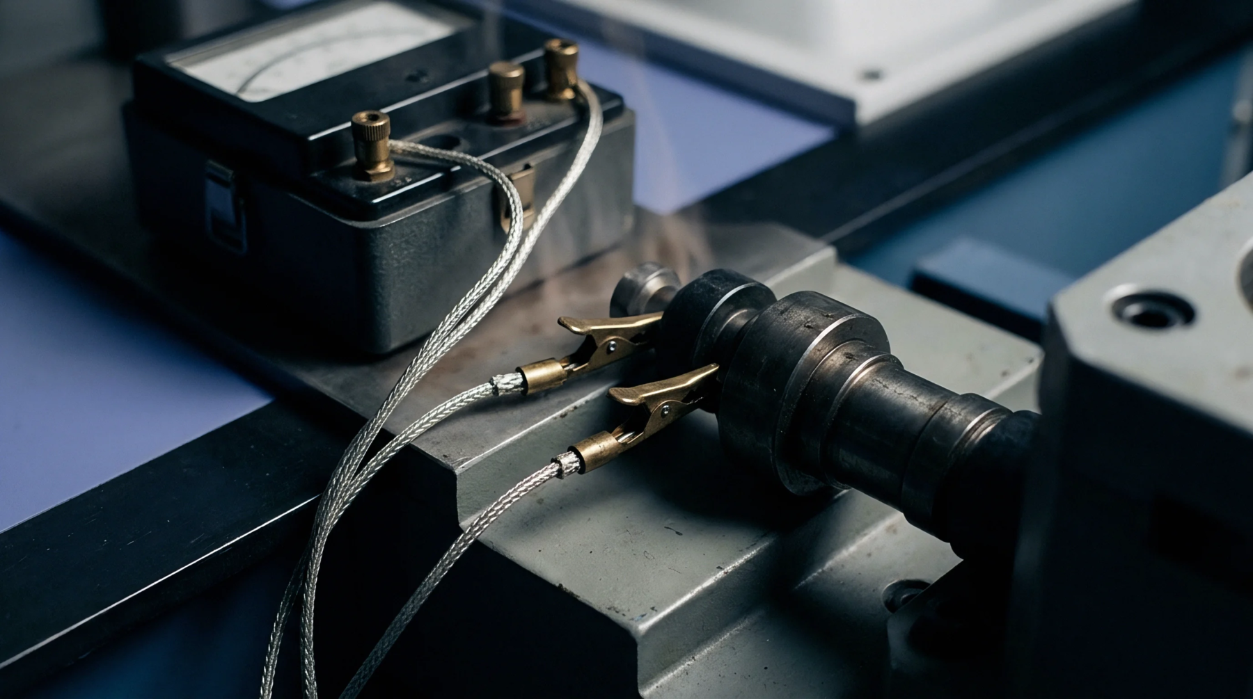
Dynamic PCB thermal gradients cause substrate flexing that alters converter resistor ladder ratios via piezoresistive strain, driving gain drift.
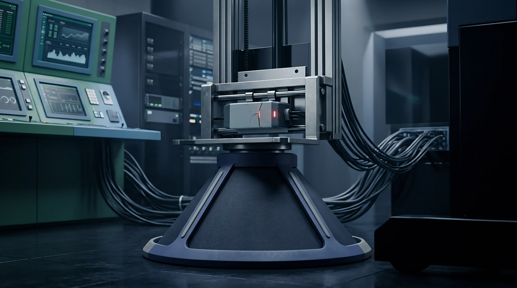
Dynamic asymmetric board strain couples into silicon piezoresistors via solder joints, causing uncompensated baseline drift mitigated by PCB isolation slots.

Asymmetric thermal gradients across precision references induce microvolt offsets through Seebeck potentials and piezo-resistive stress imbalance.

Component obsolescence decisions require balancing upfront board redesign NRE against multi-year nitrogen storage capital tie-up and solderability decay risks.

Structure IC orders using exact full-reel increments matching historical baseline entitlements to bypass automated shortage allocation cuts.

Fine-pitch iso-die variants exhibit divergent zero-point offset drift governed by package compliance, substrate CTE mismatch, and mechanical piezoresistive stress transfer.

Wafer bank conversion agreements convert raw iso-die into multi-form sensor packages, shifting supply risk while managing lead time, yield, and bus drift.

Wafer level sensor package strain mitigation relies on compliant redistribution layers, optimized pad geometries, and firmware offset calibration to ensure operational stability.
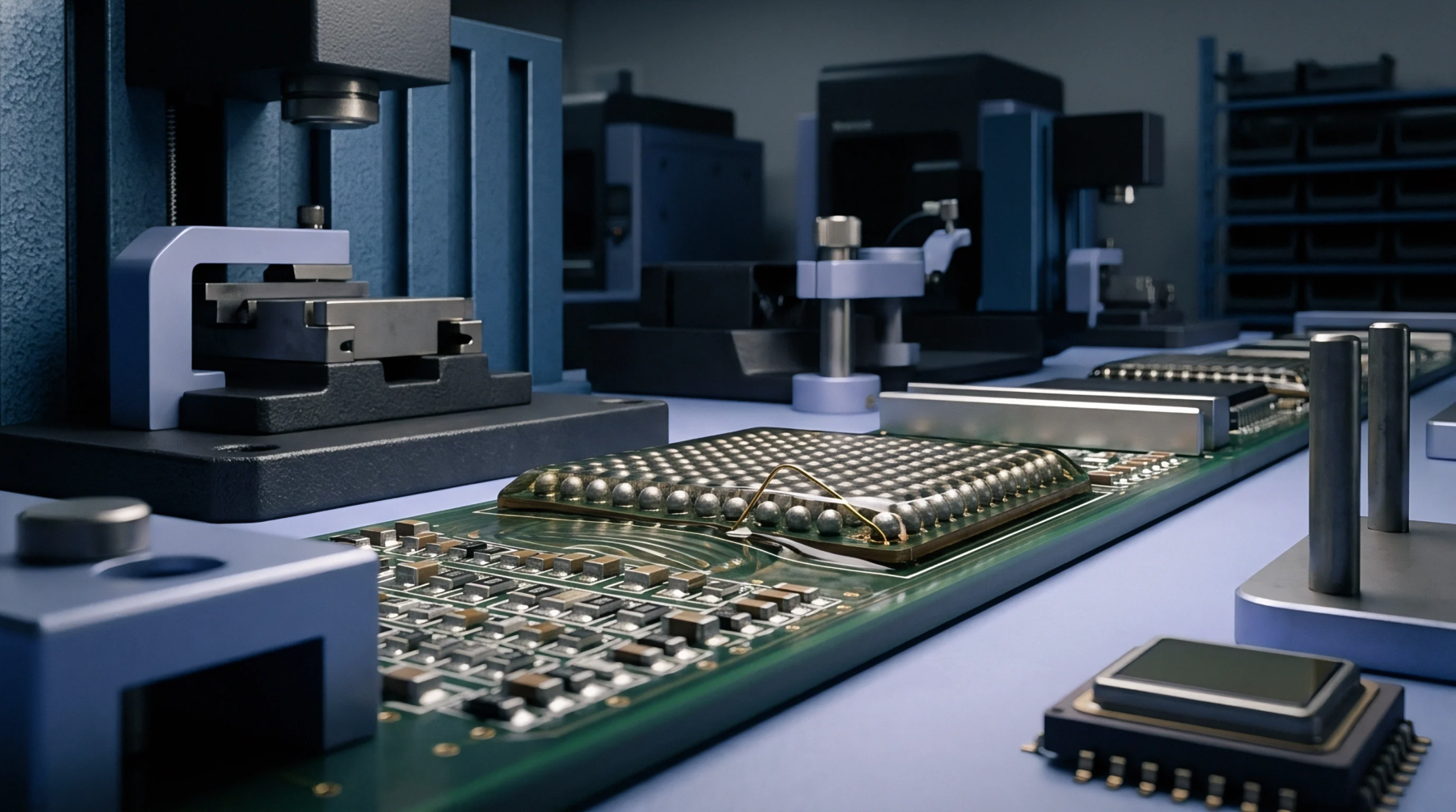
Calculated land pattern dimensions matching IPC-7351 guidelines balance solder fillet volume and placement tolerance to prevent joint stress and yield loss.
Driver self-heating creates thermal gradients across integrated precision references, causing microvolt drifts that demand symmetrical PCB layout.

Land pattern geometry, bus capacitance control, and driver timing dictate assembly yield and operational stability across sensor package formats.
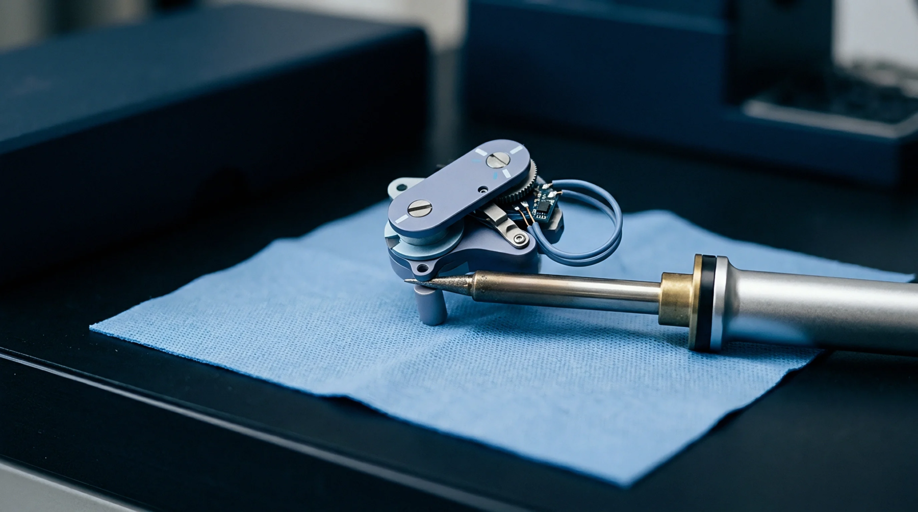
Transitioning to leadless packages reduces lead inductance by 80 percent, accelerating edge rates and requiring layout tuning to control ringing and drift.

Iso-die package selection dictates backend lead times from 4 to 20 weeks and MOQs up to 50k units, requiring total landed cost models over raw component price.

Sourcing sensor modules eliminates 4 to 12 weeks of driver engineering, flipping break-even economics below 15,000 units despite higher unit BOM prices.

Driving current from an analog sensor output heats internal silicon sub-circuits, creating thermal gradients that drift the internal voltage reference beyond nominal tolerances.
Expertise is a utility, not a secret. sentiention™ publishes its working knowledge as open reference: intelligence layer covering the materials it sources, the markets it enters, and the reference that serves both.