
IEEE 1838 Die Register Verification Protocols across High Density Interposer Bumps
IEEE 1838 die register verification across high-density interposer bumps requires cycle-accurate scan patterns mapped to low-skew DWR and FSI boundary registers.
IEEE 1838 die register verification across high-density interposer bumps requires cycle-accurate scan patterns mapped to low-skew DWR and FSI boundary registers.

Automated boundary scan architecture isolates microbump faults inside multi-die packages, replacing physical probing to safeguard assembly yields.
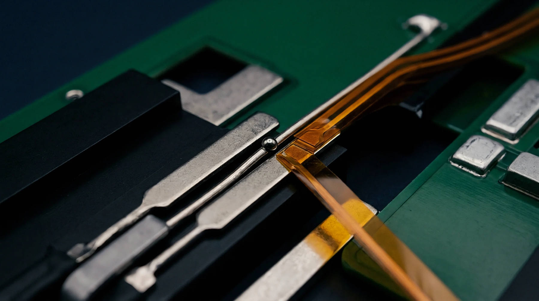
Automated pre-placement socket interrogation of silicon revision registers prevents unannounced wafer steppings from halting high-volume SMT production lines.

Validate I2C revision registers at incoming inspection to detect unannounced stepping changes and package bitfield shifts before boards reach reflow.

Surface mount sensor stepping verification relies on querying internal silicon revision registers over digital buses during automated board testing.

Viscoelastic mold compound relaxation during thermal cycling alters sensor die stress, causing unrecoverable analog drift unless modeled via Prony series.

Post-reflow zero-point drift stems from package-to-board thermal expansion mismatch, demanding compliant leads or post-assembly firmware calibration.
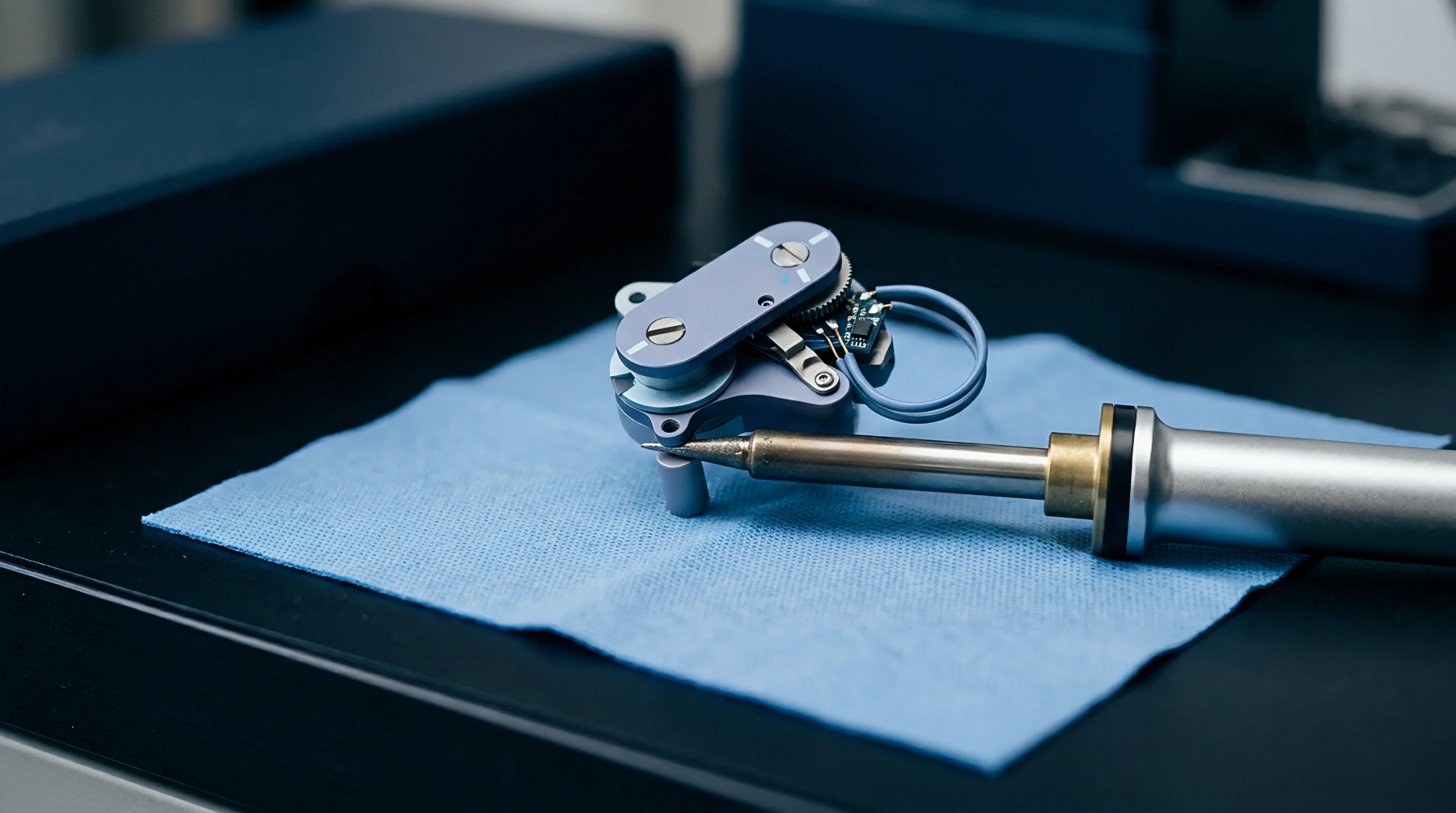
Thermal expansion mismatch in fine-pitch packages concentrates shear strain in outer joints, demanding matched underfill and strict standoff control to survive.

Unpassivated wafer conversion packaging transfers mold compound reflow stresses directly into analog trim circuits, shifting factory register offsets.

Wafer bank conversion bypasses front-end fab cycles but introduces multi-week packaging queues and compounding yield losses that inflate delivered component costs.
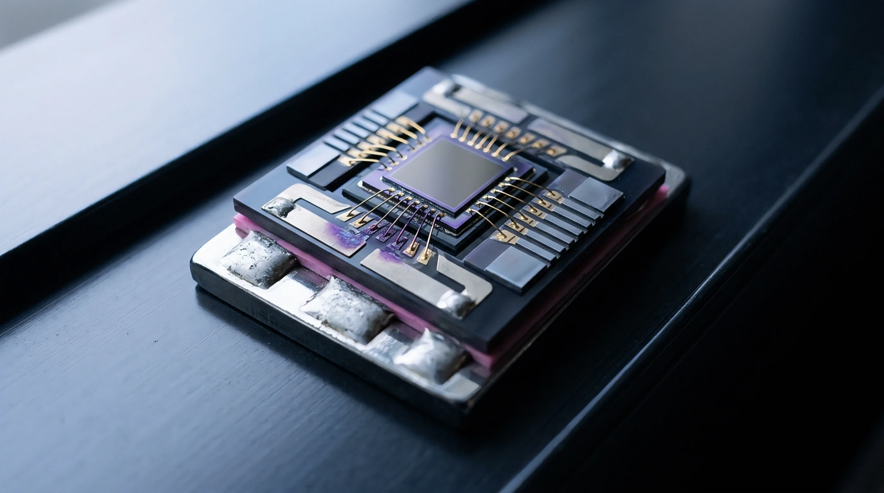
Sensor package selection fixes mechanical strain, driver stability, and break-even volumes before procurement issues purchase orders for alternative parts.

Mitigate high-modulus gel interfacial shear by combining silane-promoted substrate adhesion, laser stress relief trenches, and dual-layer modulus gradients.

Post-assembly thermo-mechanical drift limits require tracking package CTE mismatch, solder standoff compliance, and viscoelastic mold relaxation across life.

Procuring sensor mold compounds requires locking down glass transition, modulus, extractable halogens, and cold chain limits to prevent die stress and drift.

Lead-free solder creep relaxes reflow shear stress at ambient storage temperatures, tilting MEMS anchors and driving uncalibrated zero drift over time.

PCB deformation shifts surface mount sensor calibration baselines by transferring mechanical strain into the die, causing severe factory yield fallout.

Control surface-mount sensor zero offset by isolating board flex with PCB relief slots, selecting low-modulus die attach packages, and balancing solder volume.

Transient logic heating shifts substrate temperatures, degrading analog front ends without spatial floorplan isolation and matched carrier selection.
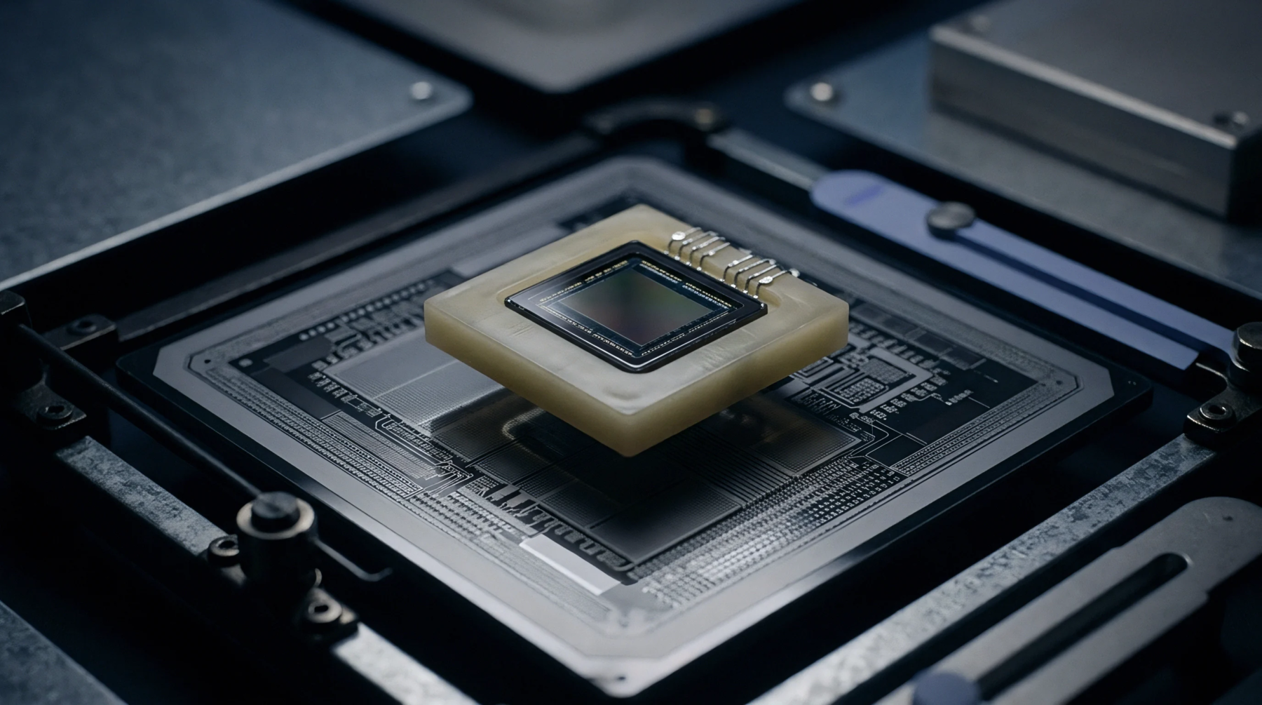
Eliminating protective mold compounds exposes silicon directly to board flexure and solder creep, driving piezoresistive offset shifts across temperature.

Silicon bandgap thermal drift inside microcontrollers creates parabolic ADC gain errors that package stress and reflow worsen, requiring careful compensation.

Evaluating package parasitics and dynamic reference drive capabilities proves vital to stabilizing dynamic conversion settlement and maximizing AFE accuracy.

Isolating large reservoir capacitors with series resistance preserves reference buffer stability while supplying instant switching charge to precision converters.

Mitigating reference droop requires low-inductance packaging, Class 1 C0G reservoirs, and high-bandwidth buffered feedback to ensure settling within conversion windows.

Package trace parasitic inductance induces millivolt ground bounce during fast transients, degrading precision reference accuracy without low-loop layout.

Dynamic reference rail settling requires low package inductance, low-ESL ceramic bypass arrays, and high-bandwidth driver buffers to prevent bit-decision errors in high-speed SAR converters.

Static DC loads on internal reference buffers induce ohmic drop and thermal feedback drift that degrade data converter accuracy past resolution limits.

Ultra-thin wafer-level sensors lose flexural rigidity at sub-100 micrometer thicknesses, transferring solder and PCB viscoelastic creep directly into active sensing elements.

Dynamic thermomechanical algorithms split pressure errors into steady polynomial drift and transient gradient terms, preserving millibar accuracy across fast thermal shocks.

Board strain transfers directly into wafer-level dies, requiring NSMD pads, stress isolation routing, or underfill to prevent fatigue and analog drift.

Modelling QFN land pattern parasitics balances via inductance, standoff capacitance, and substrate dielectric choices to maintain high-speed interface signal integrity.
Expertise is a utility, not a secret. sentiention™ publishes its working knowledge as open reference: intelligence layer covering the materials it sources, the markets it enters, and the reference that serves both.