
Analytical Shear Lag Modeling for Strain Transmission into Bottom Terminated Packages
Analytical shear lag models quantify strain transfer from boards to bottom-terminated packages, showing compliant die attach drops offset drift by 98 percent.
Analytical shear lag models quantify strain transfer from boards to bottom-terminated packages, showing compliant die attach drops offset drift by 98 percent.

Multi-channel sensor integration on standard two-wire buses demands balancing parasitic bus capacitance, address resolution, layout geometry, and landed unit cost.

Fine-pitch package assembly requires pairing stencil foil reductions with thin outer-layer dielectrics to maintain solder transfer and controlled impedance.

Asymmetric thermal expansion shifts bandgap voltage via piezoresistive substrate stress; mechanical slots and ceramic packaging isolate critical reference nodes.

Dynamic PCB thermal gradients cause substrate flexing that alters converter resistor ladder ratios via piezoresistive strain, driving gain drift.

Structure IC orders using exact full-reel increments matching historical baseline entitlements to bypass automated shortage allocation cuts.

Fine-pitch iso-die variants exhibit divergent zero-point offset drift governed by package compliance, substrate CTE mismatch, and mechanical piezoresistive stress transfer.

Land pattern geometry, bus capacitance control, and driver timing dictate assembly yield and operational stability across sensor package formats.

Transitioning to leadless packages reduces lead inductance by 80 percent, accelerating edge rates and requiring layout tuning to control ringing and drift.

Iso-die package selection dictates backend lead times from 4 to 20 weeks and MOQs up to 50k units, requiring total landed cost models over raw component price.

Precision land pattern design balances component manufacturing tolerances against board assembly capability to eliminate thermomechanical stress on silicon die output registers.

Driving current from an analog sensor output heats internal silicon sub-circuits, creating thermal gradients that drift the internal voltage reference beyond nominal tolerances.
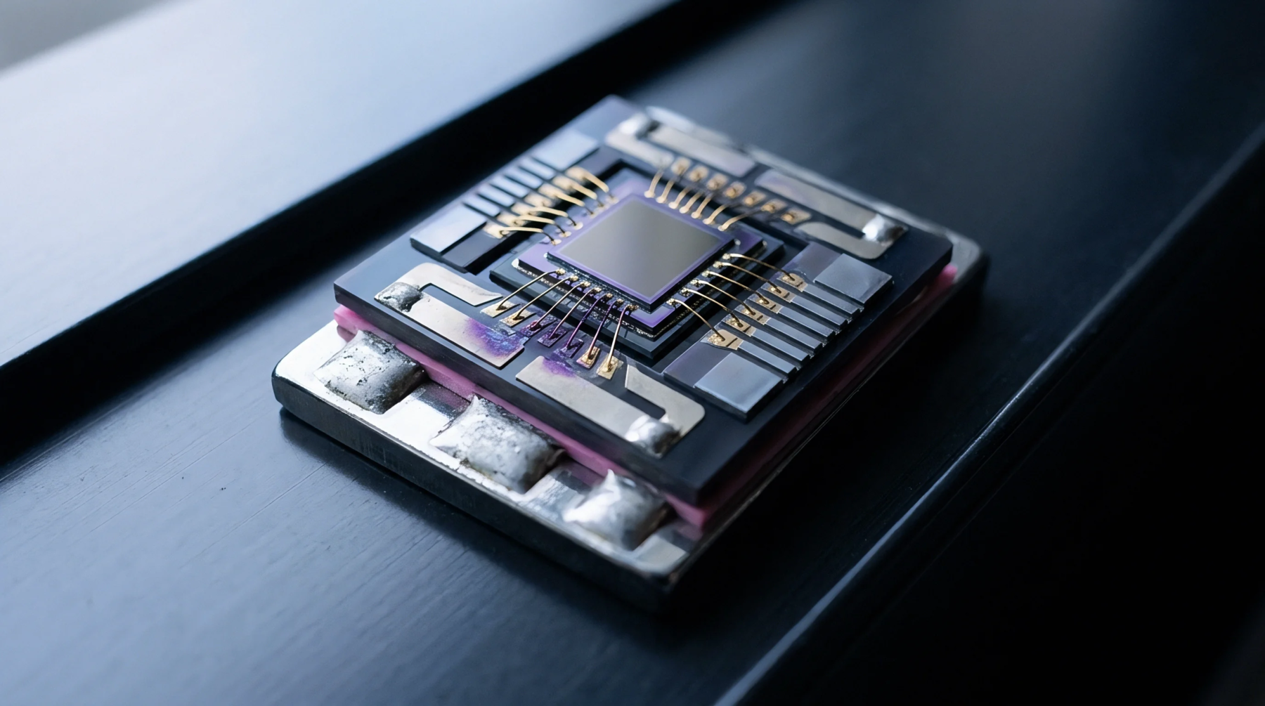
When component vendors end leaded packages, identical active silicon dies often survive in surface-mount forms that demand revised land patterns and thermal layouts.
Expertise is a utility, not a secret. sentiention™ publishes its working knowledge as open reference: intelligence layer covering the materials it sources, the markets it enters, and the reference that serves both.