
Master Supply Agreement Drift Limits and Microelectronic Acceptance
Master supply agreements enforce microelectronic acceptance by establishing guard-banded drift boundaries that partition thermal, packaging, and aging errors.
Master supply agreements enforce microelectronic acceptance by establishing guard-banded drift boundaries that partition thermal, packaging, and aging errors.

Mitigate bandgap thermal stress errors using compliant leaded packages, PCB isolation slots, polyimide die buffers, and stabilized factory calibration.

Cross-quad common-centroid bandgap layouts cancel linear thermal gradients, while PCB isolation slots prevent package piezoresistive strain from shifting Vbe drift.

Silicon piezoresistive thermal offset stems from resistor TCR imbalances and package thermal stress, requiring targeted drive excitation and polynomial compensation.

Common centroid transistor layouts for bandgap cores cancel linear thermal and lithographic gradients, reducing post-packaging output drift below 5 ppm per C.

Monolithic reference thermal drift sensitivity combines silicon junction non-linearities, piezoresistive mechanical package stress, and solder reflow hysteresis.

Heavy boron doping above 1e19 cm-3 stabilizes piezoresistive gauge factor thermal decay, allowing passive current-bias drift compensation.

Fine-pitch iso-die variants exhibit divergent zero-point offset drift governed by package compliance, substrate CTE mismatch, and mechanical piezoresistive stress transfer.
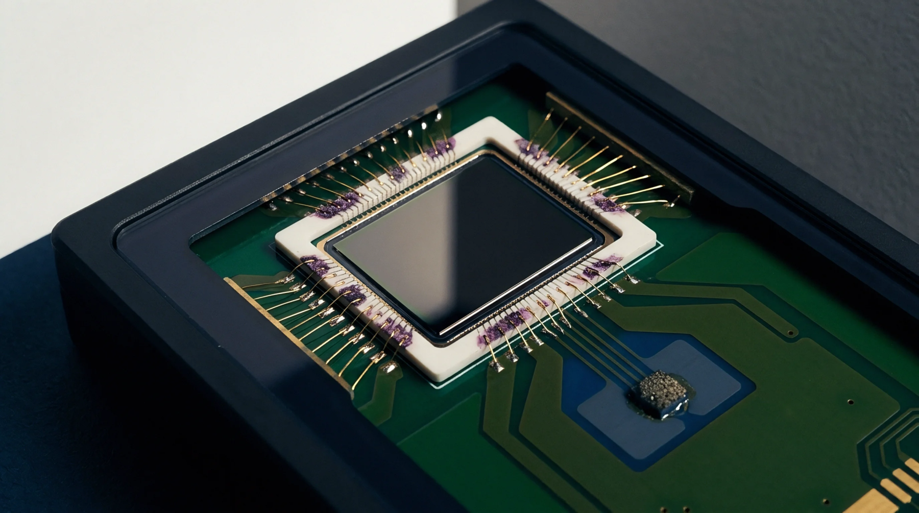
WLCSP packages transfer board thermal strain directly to the die, causing reference drift, while ceramic cavity housings eliminate mechanical coupling.

Substrate CTE mismatch drives interfacial shear strain into current shunt alloys, causing piezoresistive thermal hysteresis that requires post-cure thermal cycling to stabilize.

Viscoelastic relaxation in polymer die attach causes time-dependent strain transfer to MEMS proof masses, driving long-term zero-g offset drift.

Transitioning to leadless packages reduces lead inductance by 80 percent, accelerating edge rates and requiring layout tuning to control ringing and drift.

Optimizing boron doping concentrations between 10¹8 and 10¹⁹ cm⁻³ balances high piezoresistive gauge factors with manageable temperature coefficient drift.

Board flexure transfers surface strain into sensor packages via shear lag mechanics, where higher standoff height and low-modulus interconnects attenuate die stress and offset drift.

Isothermal precision reference layouts eliminate microvolt thermal EMFs and mechanical strain by balancing copper symmetry, milling strain-relief cuts, and decoupling heat flow.

Mechanical strain alters piezoresistive die Wheatstone bridge resistance, producing analog offset voltages that propagate through gain stages into digital register counts.

Asymmetric output load dissipation creates substrate thermal gradients across monolithic reference dies, inducing microvolt baseline offsets in precision data converters.

P-type silicon piezoresistors doped with boron to 1e18 cm-3 achieve an optimal balance between gauge factor magnitude and thermal coefficient stability.

Viscoelastic relaxation in organic sensor die attach adhesives causes baseline zero drift that requires thermal pre-conditioning bake cycles to stabilize.

Optimizing piezoresistive sensor wafers requires targeting acceptor doping between 1x10^18 and 3x10^18 cm^-3 to balance gauge factor against thermal drift.

Substrate thermal expansion creates packaging shear stress that warps MEMS proof masses, demanding central single-anchor isolation and polynomial offset calibration.

Silicon piezoresistive strain sensitivity depends on boron doping density, requiring constant current excitation or bivariate digital polynomials to suppress thermal span drop.

Substituting high-grade physical sensors with multi-element algorithms saves unit cost but adds firmware overhead, thermal drift risks, and qualification expenses.
Expertise is a utility, not a secret. sentiention™ publishes its working knowledge as open reference: intelligence layer covering the materials it sources, the markets it enters, and the reference that serves both.