
Fixed Point Polynomial Matrix Compensation for Temperature Dependent Sensor Drift
Fixed-point polynomial matrix compensation resolves cross-axis thermal drift on integer microcontrollers by balancing Q-format scaling against package stress.
Fixed-point polynomial matrix compensation resolves cross-axis thermal drift on integer microcontrollers by balancing Q-format scaling against package stress.
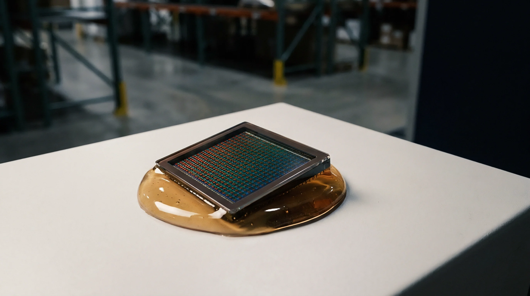
Silicon strain sensor thermal offset drift stems from piezoresistor TCR mismatches and package thermomechanical stress, resolved by digital ASIC compensation.

Tensorial stress analysis maps dynamic reflow shear and peel forces across package substrates to prevent non-wet opens and mitigate board-level solder cracking.

Optimal ASIC register tuning balances front-end gain against polynomial resolution, minimizing thermal offset and span drift across packaging stress limits.

Viscoelastic mold compound relaxation and PCB flexure shift bandgap reference voltages via silicon piezoresistivity, demanding thermomechanical co-simulation.
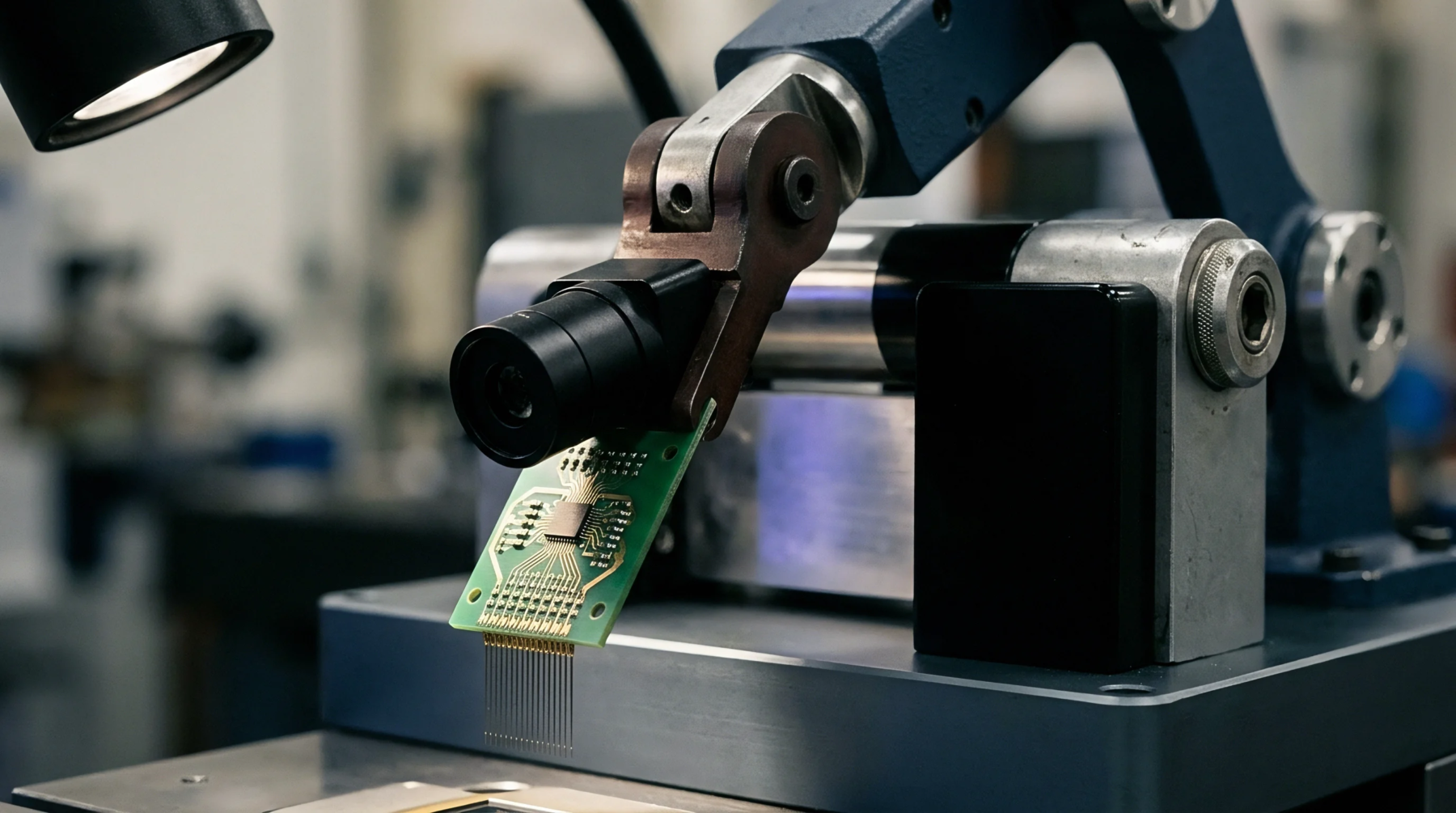
Full-bridge piezoresistive layouts linearize strain response and reject thermal drift, while digital front-end packages shift line calibration into firmware.
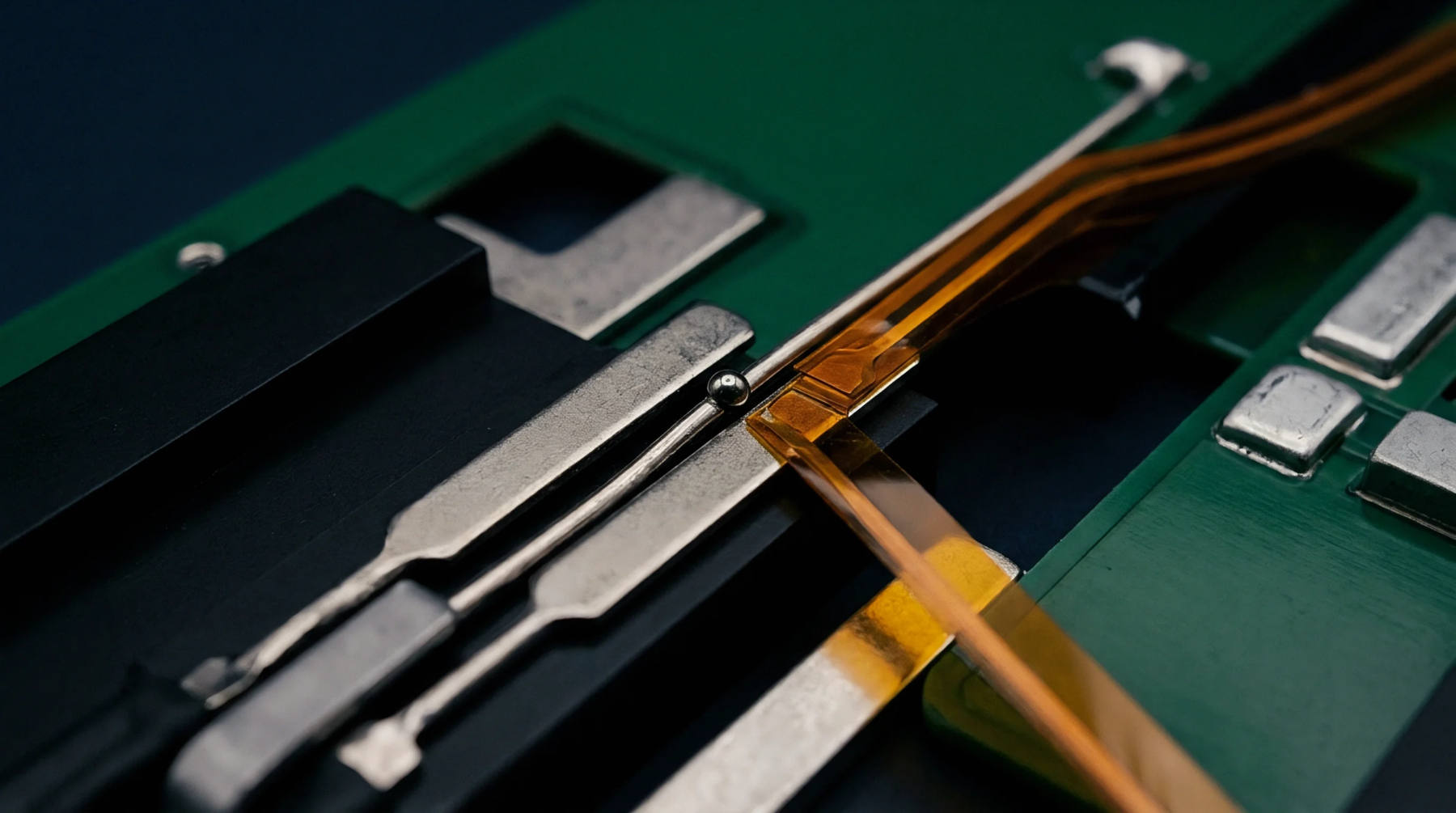
Asymmetric PCB expansion forces differential shear across bandgap die pairs, requiring balanced land patterns and isolation slots to preserve millivolt precision.

Packaging mold shrinkage and board reflow solder strain alter silicon bandgap voltages via piezoresistive coupling, demanding compliant leads or ceramic packages.

Anisotropic silicon strain tensors corrupt precision converter references; selecting compliant leadframes or ceramic cavities prevents uncorrectable drift.

Dynamic PCB thermal bending moments induce false piezoresistive bridge drift that layout slots, compliant leadframes, and synchronous sampling resolve.

Milled PCB isolation slots and compliant leaded packages attenuate board-level thermal gradient strain to preserve 24-bit converter offset accuracy.

Intermetallic growth stiffens the solder substrate interface, converting creep strain into high interfacial shear stresses that accelerate thermal fatigue failure.

Calculate viscoelastic stress transfer by fitting multi-mode Prony series DMA data and applying Arrhenius-corrected shift factors under thermal cycling dwells.

Surface mount packaging transfers printed circuit board flexure to piezoresistive silicon dies, causing bridge zero shifts that defeat digital compensation.

Post-package bandgap voltage reference drift stems from mold compound thermal strain and moisture swelling, requiring ceramic packaging or stress-isolated PCB layouts to maintain sub-10 ppm accuracy.

Orthogonal cross-quad bipolar layout cancels linear packaging stress and inverts shear vectors to stabilize bandgap reference drift below two millivolts.

Common-centroid cross-quad transistor layout and symmetrical thermal isolation eliminate systematic process gradients to hold sub-millivolt reference accuracy.

Dynamic asymmetric thermal cycles induce unrecoverable solder creep that relaxes packaging stresses, shifting precision sensor baselines over operating time.

Substrate warpage injects mechanical strain directly into the sensing die, shifting analog front-end bridge balance past digital trim limits.

Board flexure and reflow strain pass straight into surface mount piezoresistive die; routing slits, soft die attach, and glass pedestals isolate zero drift.

Dynamic micro-thermal gradients across dissimilar package metals induce Seebeck drift that common-centroid routing and ceramic substrates minimize.

Balanced copper layout and symmetric isolation slots eliminate cross-die thermal gradients, suppressing uncompensated voltage drift in surface-mount references.

Precision voltage references demand symmetric copper lands, isolation slots, and convective shielding to suppress piezoresistive and thermoelectric drift.

Plastic sub-bandgap references shift up to 300 ppm across thermal cycling due to mold compound viscoelastic creep, requiring mechanical keep-outs or ceramic forms.
Minimizing reference drift requires non-solder-mask-defined pads, compliant gull-wing packages, and perimeter routed slots to isolate circuit board strain.

Bandgap output voltage temperature coefficients balance complementary and proportional silicon junctions, shifting under package stress and thermal hysteresis.

Nonlinear hydrothermal coupling drives delamination through 4.7 MPa vapor pressure, depressed resin Tg, and CTE mismatch, causing permanent sensor offset drift.

Dual stage Carter Kibler diffusion modeling predicts bound moisture retention and prevents catastrophic package popcorning during high temperature surface reflow.

Non-Fickian moisture sorption causes delayed polymer relaxation, elevating trapped internal water mass and triggering catastrophic reflow delamination.

Hygrothermal interfacial stress calculation requires superimposing thermal mismatch stresses, moisture expansion swelling forces, and internal vapor pressure.
Expertise is a utility, not a secret. sentiention™ publishes its working knowledge as open reference: intelligence layer covering the materials it sources, the markets it enters, and the reference that serves both.