Precision Analog Reference Drift Mitigation under Thermal Stress
Mitigate reference thermal drift by isolating footprints with milled PCB slots, enforcing post-reflow stabilization bake, and selecting ceramic packaging.


Anchor

Reflow Shift and Thermo-Mechanical Strain Coupling
Precision voltage references encounter their most severe operational disturbance before the circuit board leaves the assembly plant. Lead-free surface-mount assembly subjects components to peak temperatures between 245°C and 260°C under IPC/JEDEC J-STD-020 standards. This thermal excursion plasticizes the epoxy mold compound, alters the internal stress field around the integrated circuit, and produces an immediate, non-recoverable output voltage shift termed soldering heat shift.
In bandgap devices fabricated on planar silicon, this uncompensated shift spans 100 parts per million to 450 parts per million. Buried Zener references housed in standard plastic packages demonstrate shifts between 50 parts per million and 150 parts per million. The magnitude of this initial offset frequently exceeds the entire five-year drift budget allocated by the hardware architecture.
The mechanism driving this shift originates in the differential coefficient of thermal expansion among the structural constituents of the packaged reference. Silicon exhibits a coefficient of thermal expansion of 2.6 parts per million per Kelvin. Standard FR-4 laminate expands at 14 to 17 parts per million per Kelvin in plane, while copper lead frames expand at 16.5 parts per million per Kelvin.
Plastic mold compounds introduce a coefficient between 10 and 25 parts per million per Kelvin below their glass transition temperature of 140°C to 160°C. Above the glass transition point, the compound expansion rate escalates to 40 to 60 parts per million per Kelvin. As the assembled board cools below the solder freezing point, differential contraction locks residual mechanical shear stress into the die face.
Copper lead frames impart asymmetrical shear stresses across active silicon surfaces through anisotropic thermal contraction.
Piezo-junction and piezo-resistive effects translate this residual mechanical stress directly into analog parameter variation. The bandgap core relies on matched current densities running through bipolar junction transistor pairs. Mechanical stress alters silicon lattice constants, shifts bandgap energy levels, and disturbs the transconductance matching of differential stages.
A compressive stress of 100 megapascals applied across a silicon die shifts the base-emitter voltage of a reference transistor by several hundred microvolts. The output drift follows the mechanical relaxation of the cured epoxy and the FR-4 substrate. This relaxation proceeds over hundreds of hours at room temperature, frustrating factory calibration protocols executed immediately after the secondary reflow stage.


Package

Lead Form Compliance and Carrier Mechanics
The physical carrier surrounding the silicon die determines how directly board-level thermo-mechanical stress propagates into the active reference circuit. Plastic Small Outline Integrated Circuit packages with gull-wing leads provide mechanical compliance through the cantilevered copper leads. Thin Shrink Small Outline Packages and Small Outline Transistor packages shorten this lead length, driving mechanical strain directly into the internal die paddle.
Bottom-terminated components like Quad Flat No-Lead devices eliminate compliant leads entirely, soldering the exposed thermal die pad directly to the printed circuit board foil. This mechanical coupling increases post-reflow output shift by a factor of three compared to gull-wing packages carrying identical silicon.
Ceramic Leadless Chip Carrier packages decouple the silicon from mold-compound expansion dynamics. Fabricated from alumina displaying a thermal expansion coefficient of 6.5 to 7.0 parts per million per Kelvin, ceramic hermetic packages eliminate the moisture absorption and subsequent swelling that plague epoxy mold compounds. The absence of an organic encapsulation medium prevents moisture-driven stresses that alter output voltages across variable humidity regimes.
However, the rigidity of ceramic bodies creates substantial solder fatigue risks when soldered to standard epoxy glass laminates without compliant corner leads. Thermal cycling from minus 40°C to 125°C concentrates strain at the castellations, leading to solder fracture or uneven stress transmission over operational lifetimes.
| Package Configuration | Mounting Footprint Area | Expansion Rate | Reflow Voltage Shift | Thermal Hysteresis |
|---|---|---|---|---|
| Hermetic TO-46 Metal Can | 28.3 mm² | 5.5 ppm/K | 15 to 45 ppm | 5 to 15 ppm |
| Ceramic LCC-8 Hermetic | 25.0 mm² | 6.7 ppm/K | 35 to 80 ppm | 15 to 35 ppm |
| SOIC-8 Gull-Wing Plastic | 31.2 mm² | 14.5 ppm/K | 120 to 250 ppm | 45 to 90 ppm |
| MSOP-8 Miniature Plastic | 15.3 mm² | 16.0 ppm/K | 180 to 380 ppm | 65 to 130 ppm |
| DFN-8 Exposed Pad Plastic | 6.0 mm² | 17.5 ppm/K | 280 to 600 ppm | 110 to 240 ppm |
Through-hole metal can configurations, specifically TO-46 and TO-99 packages, isolate the die from board flexure and laminate shear forces. The three or four kovar leads elevate the sealed header above the printed circuit board, converting board-level deflections into minor bending moments along flexible wire leads. The silicon die bonds to an internal header platform sealed under dry nitrogen with a welded metal cap.
This construction shields the active junction from external atmospheric moisture, surface contaminants, and assembly torque. The trade penalty involves automated assembly incompatibility, manual insertion labor, vertical volume consumption, and substantially elevated component unit costs.

Why Do Plastic Mold Compounds Induce Thermal Hysteresis?
Thermal hysteresis defines the non-repeatability of an analog reference output voltage when subjected to a complete thermal excursion cycle. When a circuit transitions from 25°C up to 85°C and returns to 25°C, the final output fails to match the initial voltage. Plastic encapsulation materials exhibit viscoelastic behavior, undergoing non-linear molecular rearrangement across temperature changes.
The mold compound does not contract along the identical physical curve through which it expanded. The silicon die experiences a different net strain state at 25°C following a cooling cycle than it experienced preceding heating.
Moisture absorption exacerbates this hysteresis. Standard epoxy mold compounds absorb between 0.15% and 0.50% atmospheric water by weight depending on ambient relative humidity. Absorbed water plasticizes the polymer matrix, lowering the effective glass transition temperature and causing volumetric swelling.
Desorption during elevated thermal testing alters the internal stress field independently of temperature. Baking an assembled board at 125°C removes moisture and alters the zero-stress baseline of the reference. Returning the unit to 60% relative humidity causes gradual swelling over weeks, creating slow analog drift that mimics long-term aging.
Silicon dies incorporate internal stress-relief features to counteract these package effects. Modern precision bandgap topologies position critical matching pairs within the central region of the die, oriented along crystal axes demonstrating minimal piezoresistive coefficients. Layout designers place active reference cores symmetrically along the neutral stress axis of the silicon chip.
Quadrature layout techniques cancel linear mechanical gradients across the active circuitry. Silicon foundries apply thick polyimide buffer coatings over the die surface prior to packaging. A 5 to 10 micrometer polyimide layer cushions the brittle silicon face against the hard silica filler particles present in transfer-molded epoxy compounds.


Relief
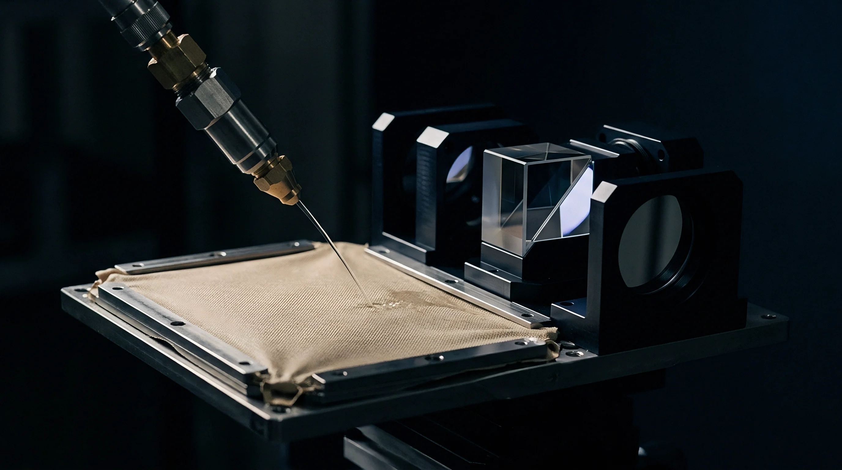
Substrate Isolation Routing and Slot Topologies
Printed circuit board layout practices directly mitigate the mechanical energy transmitted from the laminate into the reference package. Board warpage occurs during normal thermal fluctuations due to unequal copper layer distributions and structural mounting restraints. When an enclosure torques an unisolated printed circuit board, bending moments project into the surface copper lands.
The reference package absorbs these strains through its solder joints. Precision performance degrades when chassis assembly or uneven thermal dissipation warps the underlying laminate.
Milling mechanical relief slots into the laminate around the voltage reference forms a compliant island that breaks strain continuity. A U-shaped routing profile surrounding three sides of the component frees the local substrate from planar board stresses. Bending moments traveling through the primary board dissipate at the slot perimeter rather than traversing the package footprint.
The tab connecting the isolated island to the host board carries only the electrical traces necessary for power, ground, and signal delivery. Routing these connections across a narrow bridge preserves mechanical compliance while maintaining necessary circuit continuity.
Stress relief strategies follow defined physical routing constraints:
- Isolation slot width holds a minimum dimension of 1.0 millimeter to accommodate standard mechanical routing tool diameters while preventing debris accumulation.
- Bridge tab connection width stays below 3.0 millimeters to maintain structural decoupling while allowing controlled escape routing for sensitive analog traces.
- Keep-out boundaries extend at least 4.0 millimeters beyond the component perimeter, prohibiting heavy copper pours, large ceramic capacitors, and through-hole fasteners within the zone.
- Trace crossing routing directs interconnections perpendicular across the narrow neck of the bridge tab to prevent diagonal tension from distorting outer land pads.
Trace geometry on the reference landing zone also governs stress balance. Thick copper pours directly anchored to component lands pull the pins unevenly as temperatures fluctuate. Each terminal of the reference package connects through symmetrical trace widths, matching thermal resistance and physical copper volume across opposing pairs.
Uneven copper distributions generate asymmetric tipping forces during reflow solder solidification, skewing the component and imparting permanent mechanical tilt. Solder mask defined pads ensure strict volumetric uniformity of the solder joints, whereas non-solder mask defined pads permit fillet variation along the trace neck.
Multilayer board stack-ups require balanced dielectric and copper layers across the vertical z-axis center line. An unbalanced stack-up curls under thermal cycling, exerting continuous vertical tension on package corners. Eliminating heavy inner-layer copper planes directly underneath the reference island prevents local thermal expansion mismatch between the FR-4 core and the reference leads.
Placing copper cross-hatching instead of solid ground planes beneath the reference landing pad lowers substrate rigidity without sacrificing essential electrostatic shielding.


Furnace

Oven Stabilization and Active Thermal Enclosures
Eliminating temperature coefficients entirely requires controlling the immediate thermal environment of the silicon. Oven Controlled Voltage References stabilize the internal reference core at a elevated temperature above the maximum ambient operating limit, typically between 85°C and 95°C. At this regulated plateau, ambient temperature shifts of 50°C generate millikelvin changes at the reference junction. The thermal control circuit utilizes a co-packaged heating element and a tightly coupled temperature sensor to regulate the core envelope continuously.
Modern integrated heated references contain the heating element, temperature sensor, and reference core within a single silicon die or a compact multi-die module. Older legacy approaches mounted discreet buried Zener dies into heated metallic enclosures. Integrated heated bandgaps reach thermal equilibrium rapidly while consuming between 25 milliwatts and 100 milliwatts of quiescent heater power under standard room conditions.
The controller drives sufficient current through internal heating transistors to counteract thermal losses to the surrounding circuit board. When external temperatures climb toward the set point, the heater throttle reduces power to maintain a constant silicon temperature.
A thermal stabilization loop maintains sub-ppm stability only while the regulated core temperature remains strictly above peak ambient operating boundaries.
Thermal isolation between the heated reference structure and the external environment dictates system energy efficiency and stability. Encapsulating the reference within an insulated plastic cover minimizes convective cooling from system fans and ambient draft currents. On-board air currents represent an overlooked noise source.
Air moving at varying velocities creates localized, fluctuating cooling gradients across the package surface. These shifting gradients produce low-frequency thermal noise in the 0.1 Hz to 10 Hz band, masquerading as electrical flicker noise in high-resolution conversion stages.
Thermal layout techniques optimize heated reference operation through specific structural steps:
- Inner layer thermal breaks isolate the component footprint by removing solid internal planes, keeping heat energy concentrated at the package location.
- Symmetrical perimeter via barriers surround the reference island, blocking lateral conductive heat transfer from adjacent power supply switching transistors.
- Miniaturized conformal baffles shield the package from forced air streams generated by system cooling fans, preventing localized draft transients.
- Extended thin tracking introduces high thermal resistance on power traces, slowing the escape of heat along external copper interfaces.
The operational penalty of heated references centers on warm-up delay and static power consumption. A precision bench instrument easily provides the requisite power and tolerates a five-minute stabilization window. Portable or loop-powered industrial instruments operating within a 4-to-20 milliamp budget cannot sustain continuous heater drive currents exceeding 10 milliamperes.
In battery-backed or low-power nodes, designers turn instead to digital compensation and factory calibration schemes to mitigate thermal excursions without expending continuous thermal energy.


Trim

Bus-Driven Digital Compensation Architecture
Digital temperature compensation bypasses the mechanical and electrical penalties of physical ovens. This methodology measures local package temperature and injects a correcting offset through an auxiliary digital-to-analog converter or via internal non-volatile trim registers. Modern mixed-signal designs link a precision digital temperature sensor directly to the host microcontroller, sampling temperature data alongside high-resolution analog conversions.
The controller calculates the expected reference error using a calibrated polynomial model, then adjusts the system gain or corrects the raw digitized output in firmware.
Calibration coefficients map the individual temperature curvature of the reference die. Standard bandgap devices exhibit an inverted parabolic drift profile over temperature, characterized by a second-order polynomial equation:
V(T) = V0 × (1 + α × (T − T0) + β × (T − T0)²)
First-order temperature coefficient α and second-order curvature term β vary between production lots. A multi-point factory calibration over temperature extracts these individual parameters for each assembled board. Storing these constants in on-board EEPROM allows the application processor to execute continuous mathematical compensation across the entire operational envelope.
This approach compresses a 20 ppm/K uncompensated bandgap reference down to an effective 1.5 ppm/K system accuracy across a minus 40°C to 85°C industrial temperature span.
| Interface Topology | Pin Count | Maximum Bus Clock | Firmware Bring-Up Effort | Thermal Isolation Risk |
|---|---|---|---|---|
| Analog Trimming Resistor | 1 Pin | Static DC | 0 Engineering Weeks | Zero Conductive Lines |
| Two-Wire I2C Digital Bus | 2 Pins | 3.4 MHz (High Speed) | 1 to 2 Engineering Weeks | Medium Copper Coupling |
| Four-Wire SPI Digital Bus | 4 Pins | 50 MHz | 2 to 3 Engineering Weeks | High Copper Coupling |
| Single-Wire Custom Pulse | 1 Pin | 100 kHz | 3 to 4 Engineering Weeks | Minimal Copper Coupling |
Digital trimming through local communications buses introduces layout considerations. Running fast digital clock and data lines directly adjacent to high-impedance reference trim terminals injects digital switching noise into the analog core. High-speed SPI lines operating with steep sub-nanosecond edge rates couple transient charges across internal package lead frames.
Interspersing analog guard traces and separating digital interface lines from sensitive reference inputs protects the system from digital clock corruption. Ground bounce on digital return lines corrupts the voltage output if digital and analog ground returns share common copper paths on the board.

Which Calibration Interval Addresses Solder Stress Recovery?
Post-assembly stabilization dictates the timing of final factory calibration runs. The thermo-mechanical stress induced during reflow cooling relaxes asymptotically over time. Calibrating an instrument immediately after it exits the wash line captures an unstable stress baseline.
Over the subsequent 168 hours at room temperature, the package mold compound and solder joints relax, moving the output voltage by 30 to 80 parts per million. Calibrating prior to this relaxation locks in an offset error that permanently degrades product accuracy.
An elevated burn-in profile accelerates this relaxation phase. Subjecting assembled printed circuit boards to 24 hours at 125°C or 96 hours at 85°C relieves internal assembly stresses, stabilizing solder microstructure and completing post-mold epoxy curing. Following the burn-in cycle, boards must normalize at nominal room ambient conditions for a minimum of 48 hours prior to factory calibration data collection.
Skipping this stabilization protocol guarantees that early field calibration drift limits will be exceeded within the initial month of customer operation.
Digital calibration cannot correct for thermal hysteresis that lacks spatial or directional consistency. If a reference exhibits 50 parts per million of random hysteresis between rising and falling thermal sweeps, a single-valued mathematical polynomial cannot map the state accurately without tracking thermal history. Tracking direction and gradient requires memory-intensive state-machine algorithms that consume firmware space and host processing bandwidth.
Designers manage this limitation by selecting package topologies demonstrating minimal intrinsic hysteresis before implementing digital trim structures.


Audit

Lifecycle Sourcing and Total Integration Arithmetic
Selecting a reference architecture requires balancing raw purchase price against total landed manufacturing costs. Sourcing a cheap plastic bandgap reference often appears economical at the bill of materials stage. However, achieving precision analog accuracy from that part demands factory calibration cycles, specialized environmental burn-in ovens, and extended firmware development schedules.
Conversely, procuring an ultra-stable ceramic or heated reference increases initial part costs while stripping days out of production cycle times and eliminating post-reflow manual rework.
A rigorous cost analysis must evaluate the financial burden of production-line thermal testing. Establishing a multi-point thermal calibration station inside a manufacturing line involves substantial capital expenditures. Thermal chambers, automated liquid-nitrogen injection systems, precision digital multimeters, and custom multi-board test fixtures generate heavy operating costs.
Running a single printed circuit board assembly through a three-point thermal soak over minus 40°C, 25°C, and 85°C adds 18 to 35 minutes of total cycle time. On a manufacturing run of 10,000 units, this testing represents hundreds of machine hours, creating a severe operational bottleneck.
| Reference Strategy | Unit Component Cost | Assembly and Test Overhead | Firmware Integration Effort | Delivered Unit Cost |
|---|---|---|---|---|
| Plastic SOT-23 Bandgap (Uncalibrated) | $0.65 | $0.15 | $0.00 | $0.80 |
| Plastic SOIC-8 Bandgap (Oven Calibrated) | $1.85 | $6.20 | $1.50 | $9.55 |
| Ceramic LCC Buried Zener (Single-Point Trim) | $8.40 | $1.10 | $0.40 | $9.90 |
| Heated Integrated Reference (Factory Calibrated) | $14.50 | $0.35 | $0.10 | $14.95 |
| Hermetic TO-46 Metal Can (Zero Calibration) | $22.00 | $1.80 | $0.00 | $23.80 |
The arithmetic in the cost comparison table reveals the hidden expenses of aggressive component price reductions. The plastic bandgap solution operating with factory multi-point calibration costs $1.85 on the bill of materials. However, test overhead and firmware amortizations drive the true delivered cost to $9.55 per board.
The ceramic LCC Buried Zener, carrying a component cost of $8.40, yields a fully burdened delivered cost of $9.90 while eliminating multi-temperature chamber runs. The ceramic device also reduces warranty reserve liabilities tied to long-term plastic relaxation in the field.
Procurement teams must audit distributor stock and minimum order quantities across divergent packaging lines. Hermetic metal can devices and high-reliability ceramic parts face extended manufacturing lead times, frequently stretching from 26 to 52 weeks during industry allocation phases. Commercial plastic packages benefit from continuous global manufacturing runs and deep supply networks, keeping lead times under 12 weeks.
Sourcing specialists protect production continuity by securing dual-source pin-compatible footprints or validating alternate package options during early board layout phases.
End-of-life notices also threaten long-term lifecycle stability. Specialized ceramic packaging lines face shrinking commercial demand as consumer-grade electronics prioritize ultra-miniature plastic encapsulation. Manufacturers occasionally obsolete ceramic or hermetic variants while continuing high-volume production of the identical silicon core in plastic MSOP or DFN formats.
An unpredicted package discontinuation forces immediate, costly board redesigns to incorporate mechanical slots or calibration routines. Writing lifetime supply commitments into procurement agreements shields the product line from forced engineering revisions.
A supplier will state that modern epoxy formulations completely eliminate solder heat shift and thermal hysteresis issues. Operational verification on the test bench repeatedly disproves that claim across all major assembly profiles.