Cumulative Damage
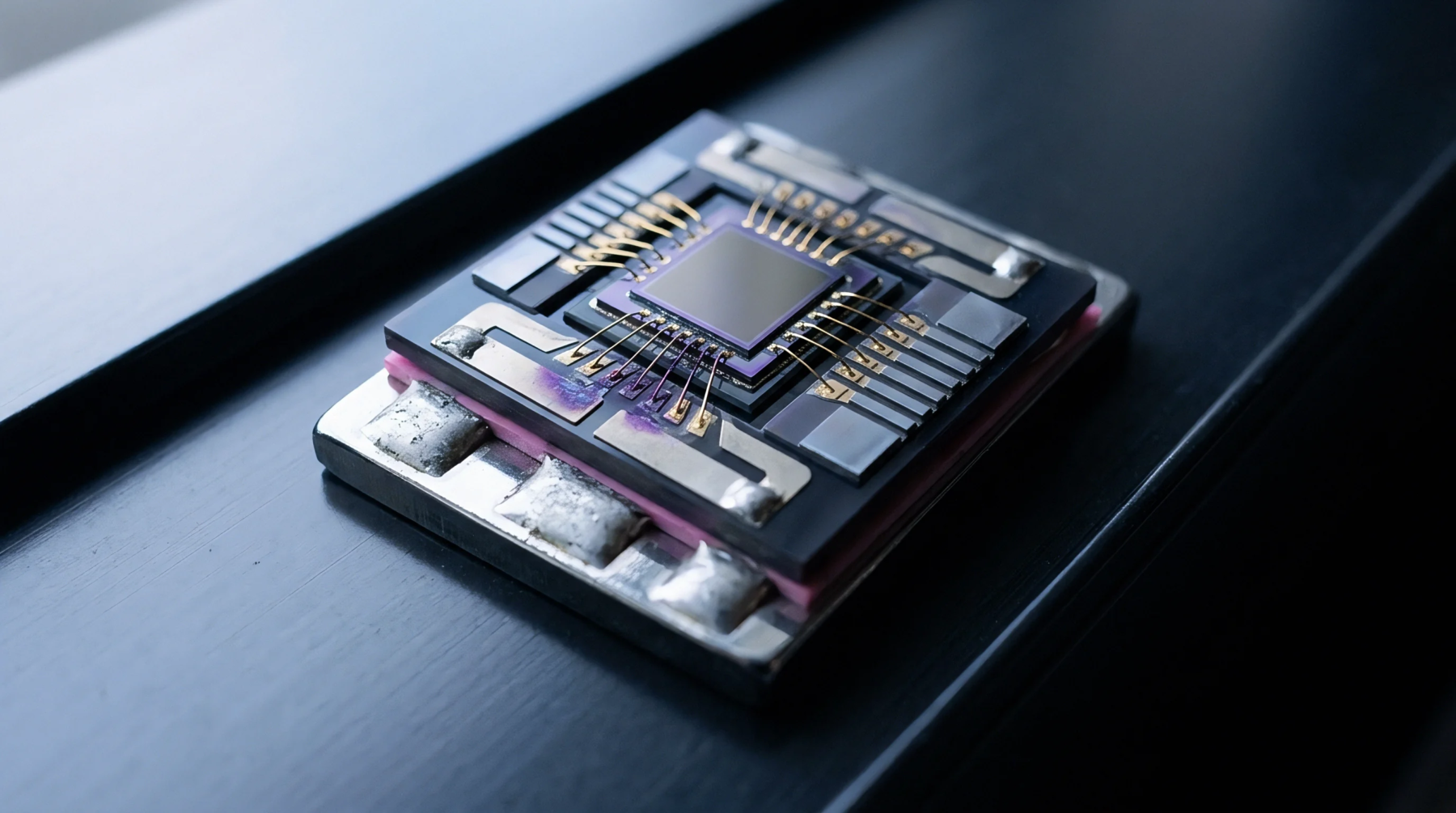
Mechanical degradation cycles involve the slow weakening of the metallic bond between a component and a circuit board due to repeated thermal expansion and contraction events. This solder joint fatigue results from differences in the coefficients of thermal expansion between the rigid silicon package and the composite material of the primary PCB substrate. Each swing in temperature causes a mismatch in movement that places a specific strain on the small grain structures of the lead-free alloy junctions at the pad level.
Over many hundreds of operations, this strain causes tiny micro-cracks to form and coalesce into larger fractures that eventually block the flow of electrical current entirely. This reliable loss of performance marks the end of life for many electronic devices that operate in harsh high-temperature cycles or outdoor installations.
Crack Initiation
Process flow of the failure starts at the molecular level where atoms rearrange themselves under stress to form slip planes inside the solidified solder mass. Solder joint fatigue accelerates when the temperature remains high for long periods, allowing the metallic grains to grow larger and become more susceptible to mechanical shear from the expanding board. As the crack begins to travel across the width of the joint, the electrical resistance of the path starts to fluctuate during the heating and cooling phases of normal use.
These intermittent connections are difficult to diagnose in the lab because they often work perfectly at room temperature while failing completely under heavy load conditions. Designers limit this risk by selecting board materials that more closely match the expansion rates of the integrated circuits themselves to lower the baseline stress level.
Thermal Geometry
Structural choices in the board layout influence how long these metallic interconnects survive before cracking wide enough to open the circuit loop completely. Larger component footprints focus more strain onto the outer solder points during expansion, making solder joint fatigue more common on the edges of large-grid-array processors or memory chips. Increasing the height of the solder stand-off provides a more compliant bridge that can absorb some of the lateral displacement before it translates into localized stress inside the metal structure.
Thin boards flex more easily than thick ones, which can actually help relieve some of the shear force in specific portable consumer electronics scenarios. However, excessive board warping during mechanical mounting will introduce new static loads that work alongside the thermal strain to speed up the initiation of internal cracks in the joints.
Qualification Limit
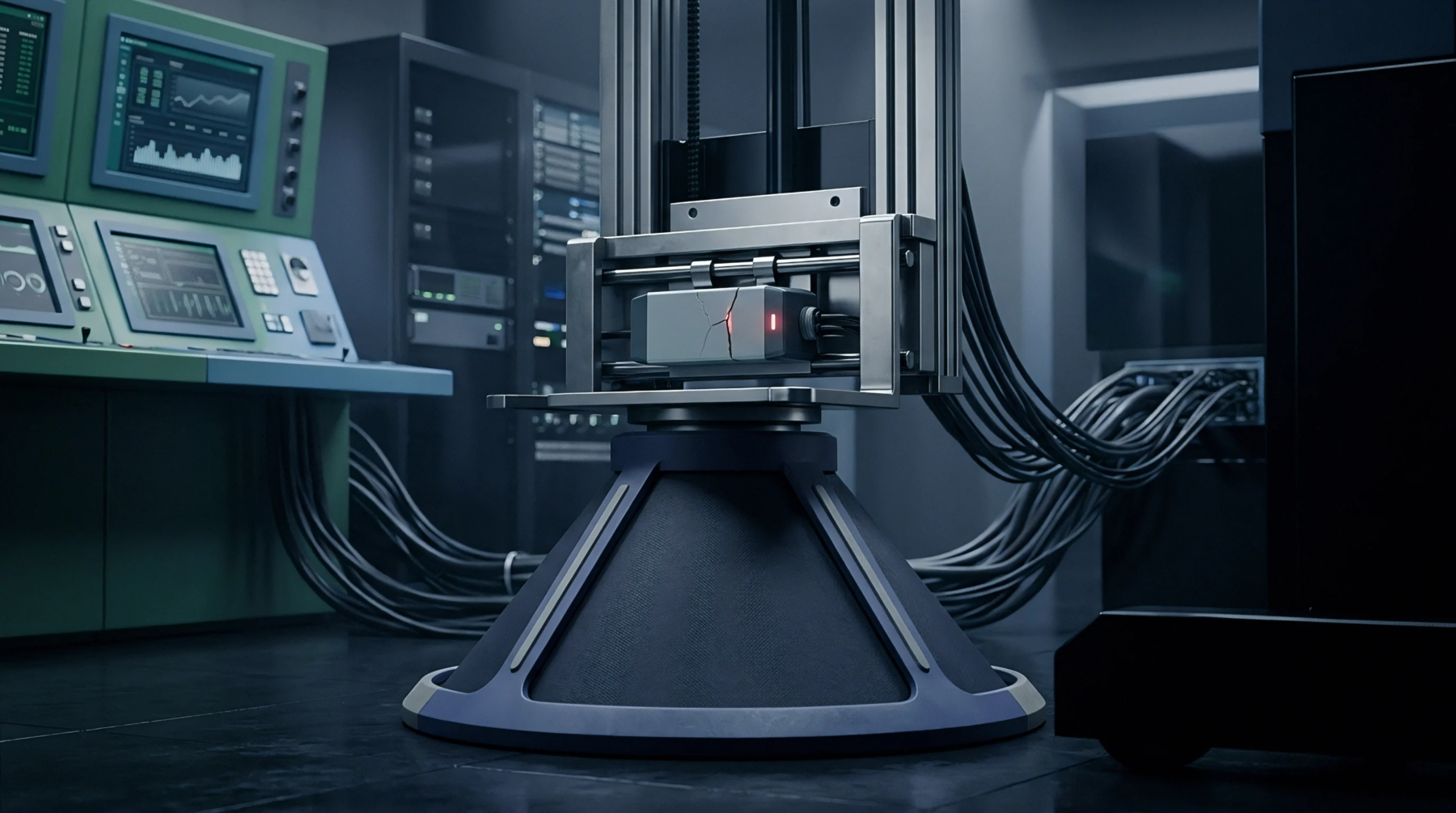
Verification of the expected reliability involves accelerated life testing where units are held in specialized chambers that swing between extremes of temperature for weeks on end. During these trials, technicians monitor individual solder sites to see exactly how many cycles can pass before solder joint fatigue triggers a detectable electrical spike or logic failure. Results are fitted to mathematical models that predict the actual survival rate in real world use cases based on the anticipated thermal profile of the end-use environment.
If the tests show early failure, the assembly strategy must shift toward using more flexible alloys or underfill polymers to shield the connections from the expansion force of the primary substrate. Consistent monitoring of these results ensures that safety-critical hardware maintains operation across its intended storage and mission spans without unexpected breakage.