Selecting Surface Mount Sensors versus Integrated Serial Sensor Modules
Discrete surface mount sensors minimize unit costs at high volume but demand board space, assembly controls, and firmware bring-up that modules eliminate.


Threshold
A bare piezoresistive pressure die in a plastic land-grid array lists at 0.82 dollars on a seven-inch tape reel, while an enclosed module carrying that exact silicon with an RS-485 transceiver lists at 16.40 dollars in tray packaging. That twenty-fold spread reflects an architectural division between component integration and subsystem procurement. Choosing between these options defines board space allocation, firmware complexity, production line tooling, and component obsolescence liabilities across the operating lifetime of a product.
A surface mount component solders directly onto the system motherboard as a bare integrated circuit or micro-electro-mechanical package. The host microcontroller assumes total responsibility for supplying filtered reference voltages, managing physical communication lines, reading raw sensor registers, and applying mathematical temperature compensation. The printed circuit assembly bears every manufacturing demand, from paste aperture sizing to post-reflow functional testing.
A module shifts calibration, signal filtering, and electrical protection from the host motherboard into the sensor vendor’s manufacturing line.
An integrated serial sensor module encases the primary sensing element alongside dedicated signal-conditioning electronics, a local processor, non-volatile calibration memory, and an industrial bus transceiver. Host controllers communicate through standardized command packets across asynchronous serial channels rather than toggling hardware registers. The package arrives pre-calibrated, temperature-compensated, and mechanically shielded against direct atmospheric contamination.

Functional Boundaries between Component and Subsystem
Hardware teams partition electronic architectures by balancing assembly cost against development schedule constraints. Surface mount sensors occupy board real estate measured in square millimeters. A typical digital accelerometer or barometric pressure sensor in a 2.0 mm by 2.0 mm Land Grid Array (LGA) footprint consumes less than 15 square millimeters of board space, including local decoupling capacitors and pull-up resistors.
Handheld devices, wearables, and compact internet-of-things nodes mandate these miniature physical outlines.
Industrial serial modules occupy substantially larger enclosures. A cabled pressure transmitter or an enclosed environmental probe housing requires mounting brackets, specialized cutouts, or external DIN-rail connections. Physical integration expands from surface-mount pick-and-place lines to manual mechanical assembly, chassis wiring, and connector mating operations.
That physical expansion isolates sensitive transducer elements from local heat sources such as power supplies, high-current microprocessors, and battery charging circuits.
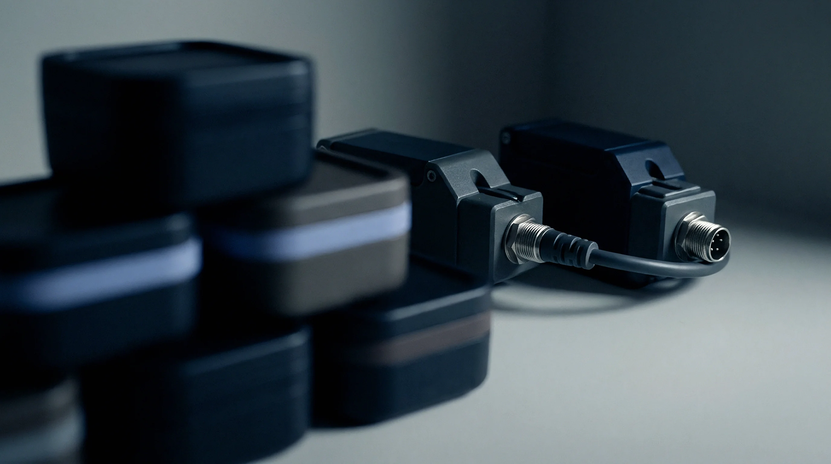
Physical Partitioning across Common Transducer Classes
Transducer physics strongly influences whether a discrete surface mount package or an integrated serial module delivers better field reliability. Environmental sensors monitoring relative humidity, volatile organic compounds, and ambient air pressure require direct exposure to the operating atmosphere. Discrete surface mount packages feature open ports or permeable membranes that invite flux residue contamination during automated solder reflow.
Serial modules isolate the sensing chamber behind sintered metal filters, waterproof membranes, or specialized flow-through channels.
Inertial and acoustic sensors present distinct mechanical coupling constraints. Accelerometers and gyroscopes require rigid mechanical attachment to the main structure to capture system dynamics accurately without attenuation. Mounting a surface mount sensor directly onto the primary circuit board couples the die to structural vibrations, but board flexure introduces baseline offset errors.
An external serial module permits mechanical isolation or dedicated dampening mounts, shielding the silicon from board-level mechanical torsion at the expense of wiring harness complexity.
| Evaluation Metric | Discrete Surface Mount Sensor | Integrated Serial Sensor Module |
|---|---|---|
| Footprint Area | 4 mm² to 25 mm² on primary PCB | 300 mm² to 2500 mm² external or daughterboard |
| Host Processing Load | Raw register reads, polling, math compensation | Parsed serial packets, engineering units |
| Bus Reach Limit | Typically < 0.3 meters (I2C / SPI) | Up to 1200 meters (RS-485 / Modbus) |
| Factory Calibration | Conducted by buyer on assembly line | Completed by supplier prior to delivery |
| Minimum Order Quantity | Tape and reel units (1,000 to 5,000 pieces) | Tray or box quantities (10 to 100 pieces) |
| Unit Price Range | $0.50 to $3.50 | $8.00 to $45.00 |
Committing to raw component placement without evaluating host processing overhead results in re-spun circuit boards and unbudgeted firmware development cycles during final system validation.


Stencil
A land-grid array package with a 0.5 mm pad pitch demands solder paste stencil apertures held to a tolerance of plus or minus 0.012 millimeters. Solder paste volume variations alter the mechanical standoff height of the package relative to the printed circuit board. That mechanical variation generates uneven shear stresses across the solder joints as the assembly cools from reflow temperatures.
Bottom-terminated components such as LGA, Quad-Flat No-Leads (QFN), and Wafer-Level Chip Scale Packages (WLCSP) leave zero clearance for visual solder joint inspection. Solder bridges form beneath blind terminations. Automated X-ray inspection becomes necessary to verify wetting and detect internal solder voiding beneath thermal and ground pads.
Voiding ratios exceeding twenty-five percent undermine mechanical stability and thermal dissipation paths.
A four-point PCB bend test at 1.2 millimeters deflection shifts bare MEMS piezoresistive bridge offsets by up to 3.8 percent of full-scale output.

Land Geometry and Solder Joint Integrity
Copper pad definitions dictate the mechanical compliance of the finished solder joint. Solder-mask-defined pads restrict paste spreading, producing consistent solder ball height but concentrating shear stresses directly along the mask edge during thermal cycling. Non-solder-mask-defined pads permit solder to wet around pad sidewalls, improving mechanical shear resistance under vibration at the expense of tighter routing channel tolerances.
Standard IPC-7351B guidelines define nominal land pattern geometries, but specialized sensors require custom stencil apertures to prevent mechanical die clamping. Pressure sensors housing micro-machined silicon diaphragms suffer baseline shifts when surrounding molding compounds experience uneven mechanical shrinkage. Type 4 or Type 5 solder pastes with spherical particle sizes between 20 and 38 microns ensure reliable release through miniature stencil apertures without clogging.

Thermomechanical Stress Transfer to Sensitive Silicon
Thermal expansion mismatches between the FR-4 circuit board substrate and the silicon sensor package transfer mechanical loads directly into the sensing structure. FR-4 exhibits an in-plane coefficient of thermal expansion between 14 and 17 parts per million per degree Celsius, whereas silicon expands at approximately 2.6 parts per million per degree Celsius. Reflow thermal profiles alter sensor zero points.
Cool-down cycles clamp the die in residual compressive stress.
Repeated thermal shock cycles between minus 40 degrees Celsius and plus 85 degrees Celsius propagate micro-cracks through lead-free solder alloys such as SAC305. The resulting stress relaxation alters piezoresistive bridge balance and capacitive gap distances inside MEMS cavities, registering as unrecoverable baseline sensor drift over time. Integrated serial modules avoid this degradation by mounting the sensing die on dedicated ceramic sub-carriers or stress-isolated internal flex circuits potted within compliant silicone gels.
Automated manufacturing lines encounter severe mechanical hazards during board assembly:
- Substrate warpage induces mechanical strain across solder balls, shifting transducer calibration curves by several percent.
- Solder bridging shorts adjacent pads beneath bottom-terminated packages when aperture ratios exceed standard limits.
- Moisture vapor explosion ruptures plastic encapsulation during rapid convection reflow cycles.
- Board flexure cracking shears ceramic substrates during panel depaneling operations.
Placing fragile sensing cavities far from high-current inductors, board mounting standoffs, and rigid structural fasteners preserves baseline calibration accuracy across the product life.

Wire
Digital communication traces routed across printed circuit boards encounter distributed resistance, inductance, and parasitic capacitance. A typical FR-4 microstrip trace introduces approximately 1.2 picofarads of parasitic capacitance per inch of trace run. Raw sensor buses operating over I2C or SPI protocols tolerate only minimal capacitive loading before signal transitions degrade.
The I2C bus specification caps total bus capacitance at 400 picofarads for Standard-Mode and Fast-Mode operations, and 550 picofarads for Fast-Mode Plus. High bus capacitance rounds off square-wave edges, violating minimum rise-time requirements and causing random clock synchronization failures. Raw register buses belong entirely within shielded enclosures, while differential serial links survive industrial factory floors.
Raw register buses belong entirely within shielded enclosures, while differential serial links survive industrial factory floors.

Where Does Bus Capacitance Break Timing Margins?
Signal rise time in an open-drain I2C bus depends entirely on the pull-up resistor value multiplied by total bus capacitance. Sizing pull-up resistors involves a compromise between edge speed and power consumption. A 2.2 kilohm pull-up resistor charging a 300 picofarad bus line yields an RC time constant of 660 nanoseconds.
This value exceeds the maximum allowable 300 nanosecond rise time defined for 400 kilohertz Fast-Mode timing.
Reducing pull-up resistance to 1.0 kilohm sharpens edge transitions but increases low-level output voltage (V_OL) and raises steady-state current draw when the line pulls low. Stray capacitance destroys fast rise times. SPI buses mitigate this rise-time limitation by using push-pull drivers, permitting clock rates above 10 megahertz, but single-ended lines radiate electromagnetic interference when routed beyond four inches without series termination resistors.

Firmware Realities and Register Abstraction
Host microcontrollers interfacing with discrete surface mount sensors must execute extensive device driver stacks. A developer writes low-level code to initialize control registers, configure interrupt masks, set output data rates, and read volatile multi-byte data registers. Silicon vendors frequently distribute pre-compiled software development kits, but integrating these libraries into custom real-time operating systems demands dedicated engineering hours.
Factory calibration coefficients stored in sensor one-time-programmable (OTP) memory require mathematical parsing on every boot cycle. A bare humidity sensor delivers raw 16-bit analog-to-digital counts. The host processor executes polynomial equations involving fourth-order floating-point operations to convert raw integers into calibrated relative humidity and temperature figures.
Host controllers absorb significant processing overhead.
Discrete component integration proceeds through a structured bring-up workflow:
- Bus line validation measures signal rise times with an oscilloscope to confirm impedance matching before applying logic analyzer probes.
- Silicon revision identification reads chip identity registers to confirm that the physical die matches published register address tables.
- Compensation coefficient extraction parses factory trim parameters from non-volatile memory into host floating-point arithmetic pipelines.
- Interrupt threshold qualification verifies data-ready pin assertion against register status polling loops to prevent missing measurement frames.
Serial sensor modules encapsulate this firmware burden behind an internal microcontroller. The module exposes a UART or RS-485 physical interface communicating via ASCII strings or binary Modbus RTU packets. The host transmits a single read command and receives processed values formatted directly in physical engineering units such as degrees Celsius or kilopascals.
Address collisions stall production lines.
| Interface Architecture | Physical Layer Type | Maximum Distance | Bus Contention Mechanism | Driver Development Effort |
|---|---|---|---|---|
| Discrete I2C | Open-drain synchronous | 0.3 meters | 7-bit or 10-bit hardware address | 2 to 4 weeks (register drivers) |
| Discrete SPI | Push-pull synchronous | 0.15 meters | Dedicated Chip Select lines | 1 to 3 weeks (state machine) |
| Module UART | Asymmetric asynchronous | 3.0 meters | Point-to-point physical connection | 2 to 4 days (packet parser) |
| Module RS-485 / Modbus | Differential asynchronous | 1200 meters | Modbus slave ID byte framing | 3 to 5 days (Modbus client) |
Factory application engineers typically defend sudden register address modifications by stating that silicon revisions preserve functional behavior while enhancing internal production yields.


Outlay
A bill of materials lists the surface mount pressure sensor at 1.40 dollars, while an integrated Modbus module carrying identical silicon lists at 14.50 dollars. An inexperienced buyer selects the discrete component solely on component price. Total landed cost involves tooling amortization, factory test labor, production yields, and calibration capital expenses.
Integrating a bare surface mount sensor requires dedicated capital equipment on the manufacturing line. Piezoresistive pressure dies, electrochemical gas cells, and infrared thermopiles exhibit initial zero-point offsets and sensitivity spreads from semiconductor wafer fabrication. Solder reflow thermal shock introduces additional mechanical offset shifts.
Direct sensing demands extensive calibration chambers.
Standard IPC-A-610 Class 3 acceptance criteria enforce strict barrel fill and solder wetting limits that eliminate low-cost contract manufacturers from contesting disputed placement yields.

Capital Expenditure in Factory Calibration Chambers
A manufacturing line calibrating discrete pressure sensors requires automated pneumatic manifolds and thermal chambers capable of stepping from minus 20 degrees Celsius to plus 70 degrees Celsius. Procuring, validating, and maintaining a high-precision multi-slot thermal calibration chamber represents an initial investment of 45,000 to 120,000 dollars. Amortizing that fixture across low production volumes drastically inflates the effective cost per placed unit.
Production cycle times multiply when assemblies sit inside environmental chambers. Reaching thermal equilibrium across a batch of fifty printed circuit boards requires fifteen to thirty minutes per temperature setpoint. Cycle time per board expands from seconds on the surface-mount placement line to hours in functional test cells.
Pre-calibrated modules eliminate factory test benches. The module supplier absorbs calibration overhead by amortizing industrial calibration rigs across millions of standardized units.

Volume Crossover Points in Total Landed Cost
The economic selection boundary between surface mount sensors and serial modules pivots on manufacturing volume. To model this dynamic, assume a design team evaluates a barometric pressure sensing node. The discrete surface mount sensor costs 1.40 dollars in bill of materials expenses, adding 0.05 dollars in pick-and-place machine time, 0.45 dollars in automated test and calibration station time, and 35,000 dollars in upfront non-recurring engineering costs for custom test fixtures and driver validation.
Tooling amortization crushes low manufacturing volumes.
The alternative integrated serial module costs 14.50 dollars at a volume of 1,000 units, 10.20 dollars at 10,000 units, and 7.80 dollars at 50,000 units. The module incurs 0.35 dollars for cable connection and chassis screw fastening, but zero dollars in calibration fixture capital expenses and minimal driver development outlay. Custom test fixtures demand heavy capital.
| Production Volume (Units) | Discrete SMD Unit Cost | Discrete Total Investment | Module Unit Cost | Module Total Investment | Cost Delta (Discrete vs Module) |
|---|---|---|---|---|---|
| 1,000 | $36.90 | $36,900 | $14.85 | $14,850 | Module saves $22,050 |
| 5,000 | $8.90 | $44,500 | $12.35 | $61,750 | Discrete saves $17,250 |
| 10,000 | $5.40 | $54,000 | $10.55 | $105,500 | Discrete saves $51,500 |
| 50,000 | $2.60 | $130,000 | $8.15 | $407,500 | Discrete saves $277,500 |
The crossover point occurs near 2,800 units under these baseline parameters. Below 2,800 units, procurement of pre-calibrated serial modules minimizes overall expenditure. Beyond 10,000 units, discrete surface mount placement delivers massive financial savings that justify custom calibration tooling.
Procurement teams managing serial module contracts require comprehensive technical documentation in the request-for-quotation dossier:
- Calibration certificate deliverables specify factory drift tolerances, calibration temperature steps, and sensor serial number tracking across lots.
- Interface protocol documentation establishes complete command byte definitions, timing response windows, and error recovery sequences.
- Thermal qualification records define operational temperature limits, thermal shock survival parameters, and seal leakage thresholds.
- Longitudinal drift warranties establish acceptable zero-point drift limits across twenty-four months of continuous field operation.
Enforcing section 4.2 of standard supply agreements binds vendors to credit manufacturing losses directly whenever batch defect rates exceed two tenths of one percent.


Revision
Semiconductor foundries continually modernize wafer fabrication lines, migrating mature mixed-signal interface dies from 180-nanometer planar lithography to 90-nanometer or smaller nodes. When a sensor vendor refreshes an internal application-specific integrated circuit (ASIC), the silicon die shrinks. The manufacturer issues a Product Change Notification (PCN) asserting form, fit, and function equivalence, yet subtle operational shifts frequently emerge.
Undocumented silicon modifications introduce unexpected timing variations. An internal analog-to-digital converter pipeline may shorten its conversion window from 12 milliseconds to 8 milliseconds, causing legacy host firmware polling loops to read corrupted data frames. Power-up state transition times shorten or extend, breaking edge-triggered interrupt handlers.
Unannounced die revisions break production firmware.
Managing Silent Silicon Updates and Register Deprecation
Direct component integration exposes host code directly to register address modifications. In automotive and industrial sectors, semiconductor manufacturing allocations shift capacity toward high-volume automotive parts, leaving specialized industrial sensors vulnerable to sudden end-of-life notices. If a discrete environmental sensor manufacturer obsoletes an LGA part, replacing it requires redesigning printed circuit board copper traces, recalculating stencil apertures, and rewriting host driver libraries.
Integrated serial sensor modules establish a layer of firmware insulation between host software and raw sensing silicon. The module vendor’s internal microcontroller interfaces with the changing silicon die, while preserving identical serial output packets across the external UART or RS-485 bus. The external host continues sending identical request bytes and receiving identical payload structures, insulating high-level systems from underlying silicon updates.

Second Sourcing across Incompatible Footprints
Discrete sensors lack physical pinout standardization. An LGA-14 accelerometer from one semiconductor manufacturer rarely shares pin assignments or land geometries with an LGA-14 component from a competing supplier. Pin 1 orientation, power rail voltages, interrupt pin assignments, and internal register map configurations diverge across competing vendors.
True dual-sourcing for discrete sensors requires layout engineers to design complex dual-footprint circuit boards or maintain separate board assembly variants.
Serial modules simplify dual-sourcing by standardizing mechanical mountings and physical communication protocols. A four-pin industrial probe housing with ground, power, RS-485 non-inverting (A), and RS-485 inverting (B) pins permits drop-in replacement across alternate suppliers. Standard Modbus RTU register mapping ensures that changing sensor hardware requires zero changes to motherboard layouts or system firmware binaries.
The open question remains whether long-term maintenance savings on frozen module firmware offset the severe bill of materials penalty across high-volume production runs.