Managing Multiple Identical I2C Devices on Shared Hardware Buses
Manage identical I2C devices by combining hardware pin strapping, pass-gate multiplexers, or inline address translators to isolate matching identifiers.


Strap
Hardwired pin assignments determine the physical baseline for resolving identical target addresses on an Inter-Integrated Circuit wiring channel. Many digital environmental sensors, six-axis inertial units, and precision analog-to-digital converters arrive from wafer fabrication with fixed base locations. Package pin limitations routinely restrict external logic selection to a single dedicated line, AD0 or ADDR.
Tying this line to ground yields one target identifier, while tying it to the peripheral supply rail yields a second. Deploying three or more identical parts on the same board layout breaks this arrangement immediately.
Several sensor manufacturers implement tri-state or quad-state decoding pins to expand the direct address pool without increasing silicon area. A tri-state pin decodes ground, supply voltage, or a direct connection to the active data line. Quad-state architectures incorporate an internal window comparator sampling a resistive divider between the supply rail and ground during power-on reset.
This comparator senses defined voltage steps, mapping a single package pad to four distinct addresses.
A thirty percent drift in external bias resistance pushes quad-state divider voltages past comparator threshold windows during cold start tests at negative forty degrees Celsius.
Strap lines draw continuous current. When designers leave address selection pins floating on designs lacking internal pull-down structures, charge accumulation induces spontaneous address hopping during thermal transients. Solder flux contamination between adjacent lands creates leakage paths on tight-pitch ball grid arrays and thin dual-flat no-leads formats.
A surface leakage current exceeding five microamperes can shift a high-impedance quad-state address node into an adjacent comparator decoding band, changing the device address mid-transaction.
Hardware Address Pin Allocation Realities
Physical package geometries dictate the mechanical boundary of address expansion. Compact land patterns like wafer-level chip-scale packages or 2.0 mm by 2.0 mm land grid arrays rarely spare more than one pin for address assignment. The remaining lands belong to power rails, decoupling returns, mechanical ground, and serial lines.
Address collisions halt bus traffic. When two peripherals answer the same seven-bit identifier simultaneously, both assert the acknowledge bit by pulling the serial data line low during the ninth clock pulse. The master controller proceeds with data retrieval under the assumption that a single sensor responded.
The resulting payload constitutes a logical AND combination of the data words driven by the competing silicon outputs. Parity checks and checksum calculations fail sporadically. Diagnosing these errors in production test fixtures demands oscilloscope captures of acknowledge transitions rather than automated software scans.
| Package Format | Pin Designation | Connection Target | Resolved Address | Quiescent Bias Current |
|---|---|---|---|---|
| DFN-8 (2×2 mm) | ADDR | GND (0V) | 0x44 | 0.0 uA |
| DFN-8 (2×2 mm) | ADDR | VDD (3.3V) | 0x45 | 0.0 uA |
| LGA-14 (2.5×3 mm) | SA0 | SDA line | 0x68 | 12.5 uA |
| LGA-14 (2.5×3 mm) | SA0 | SCL line | 0x69 | 14.0 uA |
| QFN-16 (3×3 mm) | ADR_DIV | 10k to VDD, 30k to GND | 0x76 | 82.5 uA |
| QFN-16 (3×3 mm) | ADR_DIV | 30k to VDD, 10k to GND | 0x77 | 82.5 uA |

Capacitive Loading on Quad State Straps
Routing address configuration traces past high-speed digital switching paths introduces capacitively coupled noise into the address latch logic. Address decoding occurs inside the peripheral silicon during the initialization sequence, typically within two milliseconds after the supply rail crosses the brownout reset threshold. Noise spikes coupled into the address pin during this window latch false target values into the peripheral controller state machine.
Engineers prevent this corruption by placing decoupling capacitors directly adjacent to high-impedance bias dividers. Adding a ten-nanofarad capacitor stabilizes the pin voltage against power distribution ripple. This added capacitance increases the settling time of the bias network.
The master controller delays initial bus polling until the RC time constant of the address bias network settles within two percent of the nominal target level. Solder bridges cause catastrophic deadlocks.
Ignoring trace spacing tolerances on high-density interconnect layers pairs address lines with switching inductors, corrupting the hardware identification vector and permanently desynchronizing downstream telemetry packets.

Switch
Bidirectional analog switches and digital bus multiplexers isolate identical targets onto discrete hardware branches. Silicon devices such as the PCA9548A or TCA9546A accept an incoming two-wire interface and route the serial lines to one of four or eight downstream channels. A control register within the multiplexer itself sits at a dedicated base address, typically within the 0x70 to 0x77 bracket.
Software commands written to this control register connect or disconnect downstream pass-gate field-effect transistors, exposing only one sensor array segment to the controller at any given instant.
Bus switches add electrical series resistance across the serial clock and serial data lines. Typical N-channel pass-gate architectures exhibit an internal on-resistance ranging between four ohms and twenty-five ohms depending on operating voltage and die temperature. This series impedance acts in combination with downstream trace capacitance, connector pins, and device input capacitances, slowing signal transitions.
Standard UM10204 mandates that total line capacitance remain under four hundred picofarads to preserve the three hundred nanosecond maximum rise time required for Fast-mode operation.
Channel selection delays interrupt handling. When multiple sensors share alert lines routed back to the host processor, an assertion on a consolidated interrupt trace requires sequential channel selection to identify the asserting silicon. The microcontroller issues an address byte, writes a bitmask byte to the multiplexer register, generates a stop condition, and then executes the peripheral read cycle.
This arbitration overhead consumes hundreds of microseconds at standard 100 kHz bus speeds.

Multiplexer Propagation Delays and Edge Rates
Distributing eight identical sensors across dedicated multiplexer segments segments total bus capacitance. Isolating long traces behind open switches prevents downstream capacitance from loading the primary master controller. Each opened channel removes thirty to eighty picofarads of parasitic capacitance from the main line, allowing the primary segment to maintain fast transition times.
The downstream channels require dedicated pull-up resistors on each isolated pair of clock and data lines. Calculating resistor values involves factoring the on-state resistance of the pass transistor alongside the pull-up supply level. If a master device sinks current to pull the clock line below the maximum low-level input threshold (VIL), the voltage drop across the multiplexer pass gate raises the apparent low level seen by the slave.
Selecting pull-up resistors with values below two kilohms creates excessive voltage drops across the switch, pushing the low-level signal above the 0.3 VDD threshold defined by the standard.
- Host bus acquisition establishes control through the generation of a start condition directed toward the multiplexer control address.
- Channel bitmask transmission commits the target downstream branch selection into the internal multiplexer control latch.
- Bus turn-off latency allows the internal pass-gate field-effect transistors to cease conduction on deselected branches, which requires up to one microsecond for complete channel isolation.
- Downstream transaction execution sends commands to the now accessible target peripheral at its native, non-conflicting hardware address.
- Subsystem channel clearing resets the multiplexer control register to 0x00 to avoid erroneous multi-branch data contention during subsequent operations.

Channel Isolation during Device Hangs
Silicon failures on peripheral sensors frequently result in the serial data line becoming latched low. A single frozen sensor holding the data line down disables an entire unbuffered copper trunk. Multiplexers equipped with hardware reset lines offer an electrical isolation method for these conditions.
The host controller detects a bus hang when the data line remains low past nine clock cycles. Asserting the active-low hardware reset pin on the multiplexer forces all downstream pass-gate switches into a high-impedance state within thirty nanoseconds. This action frees the upstream master lines immediately, permitting communication with other critical system devices while fault-recovery software isolates the failed branch.
Field component fabricators state that pass-gate leakage current under elevated junction temperatures remains too low to influence bus logic thresholds on unselected channels.

Offset
Translating target identifiers directly at the physical interface layer eliminates the control commands needed by multiplexer switches. Active address translation ICs sit inline between the master bus and the target peripheral. Devices in this category intercept the seven-bit address byte immediately following a start condition, compare the incoming bits against an internal reference, and toggle their output drivers to present an altered address to the local slave device.
Hardware translation operates at wire speed. The translating silicon receives the incoming address bits transmitted by the host, calculates a hardware-configured XOR shift, and restructures the bits transmitted down the secondary stub. The downstream slave device recognizes its hardwired address, while the upstream host controller addresses the node using an entirely different numerical identifier.
The entire translation cycle occurs within the standard bit timing of the serial clock line.
A rule of thumb dictates that address translation buffers belong on board layouts where firmware modification is strictly prohibited by safety certification boundaries.
Level shifting introduces propagation skew. Active translators introduce a delay between the master clock edges and the slave response, typically measuring between fifty and one hundred twenty nanoseconds. In high-speed systems running at 1 MHz or 3.4 MHz, this propagation delay consumes a substantial percentage of the data setup time window (tSU;DAT).
Pull-up sizing demands strict attention to avoid rounding signal edges across translators.

Address Translation via Voltage Dividers
Translators like the LTC4316 establish their target address offset through external resistive dividers attached to dedicated analog input pins. Two external resistors form a divider network between the supply rail and ground, setting an analog reference voltage. During start-up, an internal analog-to-digital converter reads this voltage and converts it into a bitwise offset byte.
Bus capacitance degrades edge rates. Designers adjust the offset by altering standard 0402 surface-mount resistor values, shifting the apparent target address across the full seven-bit space. This hardware-centric approach requires no software driver changes within the host microcontroller.
The operating system talks to multiple identical sensors as if they were fabricated with distinct factory addresses, preserving continuous data streams without multiplexer channel switching.
| Evaluation Metric | TCA9548A Multiplexer | LTC4316 Address Translator | Secondary Hardware Controller |
|---|---|---|---|
| Downstream Devices Supported | 8 branches | 1 device per IC | Dedicated bus limit |
| Operating Current (Active) | 22.0 uA | 1.5 mA | 280.0 uA |
| Series Path Impedance | 15 ohms | Active Buffer | Zero (independent) |
| PCB Area Footprint | 31.5 mm² (TSSOP-24) | 9.0 mm² (DFN-10) | Microcontroller Pins |
| Software Driver Overhead | Channel selection writes | None (transparent) | Multiple I2C instances |
| Failure Isolation | Isolates hung channels | Isolates single node | Isolates entire bus |

Inline Translation Buffer Power Draw
Active address translators draw constant operating current to power their internal comparators, analog-to-digital sampling blocks, and logic XOR arrays. A standard eight-channel analog multiplexer consumes less than thirty microamperes in standby. A dedicated address translator consumes between one and two milliamperes during active bus transactions.
In battery-operated designs requiring multi-year operational spans, this current differential represents an important battery budget factor. When eight translators sit on a shared board to resolve identical environmental sensors, their collective quiescent draw reaches twelve milliamperes if not gated by high-side load switches. Designers must weigh this battery depletion against the processing cycles saved by eliminating multiplexer management code.
Secondary buses increase trace density.
The question of whether inline translators can maintain signal integrity over extended ribbon cables when driving mismatched branch impedances remains open among production hardware engineers.


Driver
Software architectures manage the operational state of shared-address peripherals through structured abstraction layers. In embedded operating systems like Linux, the kernel provides native client multiplexing through the i2c-mux subsystem. This framework models a multiplexer device as an arbitrator that instantiates virtual adapter numbers for every downstream branch.
Device tree declarations bind individual peripheral drivers to these virtual adapters, hiding the underlying channel selection mechanics from application software.
Application programs initiate standard read and write calls to the virtual bus adapter. Before the low-level peripheral driver initiates communication, the kernel multiplexing core acquires a lock on the parent bus. It then issues an address selection command to the multiplexer hardware, verifies the acknowledge bit, and releases the transaction lock to permit the peripheral driver to execute its data exchange.
Under typical operating conditions with an eight-channel switch, software arbitration adds up to twelve percent bus utilization overhead purely through multiplexer address selection frames.
State machine recovery requires deterministic timing. When a peripheral locks up during a transaction, the software stack cannot simply cycle the target driver. The lockup holds the serial data line low across the entire active virtual adapter, preventing the kernel from addressing the multiplexer to switch channels.
Unresolved bus states drain batteries.
Kernel Subsystem Arbitration of Shared Slaves
Embedded systems lacking multi-threaded operating system kernels must implement bare-metal scheduling loops to manage channel switching. In these architectures, non-blocking state machines poll identical sensors sequentially. The firmware tracks the active branch in an execution context block.
If an interrupt fires from a sensor on an inactive channel, the scheduler must complete the in-flight read on the active channel, issue a deselect command to the switch, reconfigure the multiplexer for the interrupting branch, and only then service the peripheral register. Interrupt latency increases dramatically under this scheme. Firmware teams handle this latency by increasing sensor internal sample buffers, reducing the frequency of hardware interrupt assertions.
- Bus deadlock timeout occurs when a target peripheral holds the serial data line low past thirty-five milliseconds, requiring clock toggling recovery.
- Arbitration loss errors surface when two asynchronous tasks attempt to configure different multiplexer branches without checking peripheral bus mutex status.
- Phantom acknowledgment events happen when an unselected branch suffers from capacitive leakage, causing noise spikes that register as valid acknowledge bits.
- Address aliasing faults develop when firmware updates alter register map pointers without synchronizing the hardware translator offset tables.

State Machine Recovery on Hanging Peripherals
Recovering a bus frozen by an identical sensor involves structured clocking routines implemented inside the low-level bus driver. When the master senses the data line stuck low, it transitions the serial clock pin from hardware peripheral control to general-purpose output mode.
The processor manual clocks the serial line up to nine consecutive times at a reduced frequency of twenty kilohertz. This clock train forces the hanging peripheral internal shift register to advance until it completes its byte transfer and releases the data line to a high state. Following the ninth clock, the processor generates a formal stop condition, driving data low and then high while clock remains high.
If this routine fails to clear the line, the firmware commands a local power switch or pulls the multiplexer reset line low. Propagation delays compound across channels.
Firmware recovery sequences succeed reliably when hardware schematics wire reset lines directly to dedicated microcontroller GPIO pins.


Yield
The selection of an address resolution architecture impacts bill of materials cost, surface-mount manufacturing yield, and printed circuit board routing complexity. Hardware address strapping represents the baseline approach, costing nothing in incremental component purchase expense. It demands negligible printed circuit board area, utilizing zero-ohm jumpers or direct copper trace ties to supply rails.
Its adoption is constrained strictly by the quantity of available address pins provided on the sensor package.
Multiplexers introduce active silicon components to the bill of materials, adding unit costs between thirty cents and one dollar twenty cents at mid-volume procurement scales. A single multiplexer package occupies surface area ranging from nine square millimeters in tiny quad flat no-lead formats up to thirty-two square millimeters in standard thin shrink small outline packages. Routing eight differential pairs of serial traces out from a central multiplexer creates wiring bottlenecks, forcing designers to add two inner copper routing layers to four-layer circuit boards.
Solder bridges between fine-pitch leads depress board assembly yields.
A production run yields fewer functional assemblies whenever fine-pitch packages require excessive manual rework to clear solder bridging beneath thermal ground pads.
Inline address translators consume nine square millimeters per monitored node. Placing six identical sensors across an automotive battery monitoring board requires six individual translator integrated circuits, multiplying the silicon cost penalty. The trace routing remains clean and linear, eliminating the star-topology wiring routes demanded by central multiplexer switches.
Board space dictates package density.

Board Area and Placement Cost Balance
Surface-mount placement machine throughput influences assembly economics. Every additional integrated circuit placed on a circuit board incurs feeder setup costs, nozzle changes, and optical alignment verification intervals. A central multiplexer adds one pick-and-place event to the manufacturing ledger.
Deploying eight discrete address translators adds eight pick-and-place events, alongside sixteen supporting bias resistors.
Inspection complexity scales with solder joint counts. Multiplexers in leadless packages require automated X-ray inspection to detect voiding and bridges under central ground slugs. Address translators in standard leaded packages allow visual automated optical inspection, reducing post-reflow inspection cycle times.
Cold joints lift during vibration.
- Direct pin strapping suits designs requiring two identical sensors situated adjacent to each other on a single rigid board substrate.
- Centralized multiplexing delivers the lowest total component cost when four to eight identical sensors sit within twenty centimeters of the main processing core.
- Inline address translation serves modular designs where identical sensor daughtercards connect to a common backplane bus without software changes.
- Multi-controller partitioning resolves high-reliability arrays by allocating groups of sensors to entirely separate hardware peripheral channels inside a high-pin-count processor.
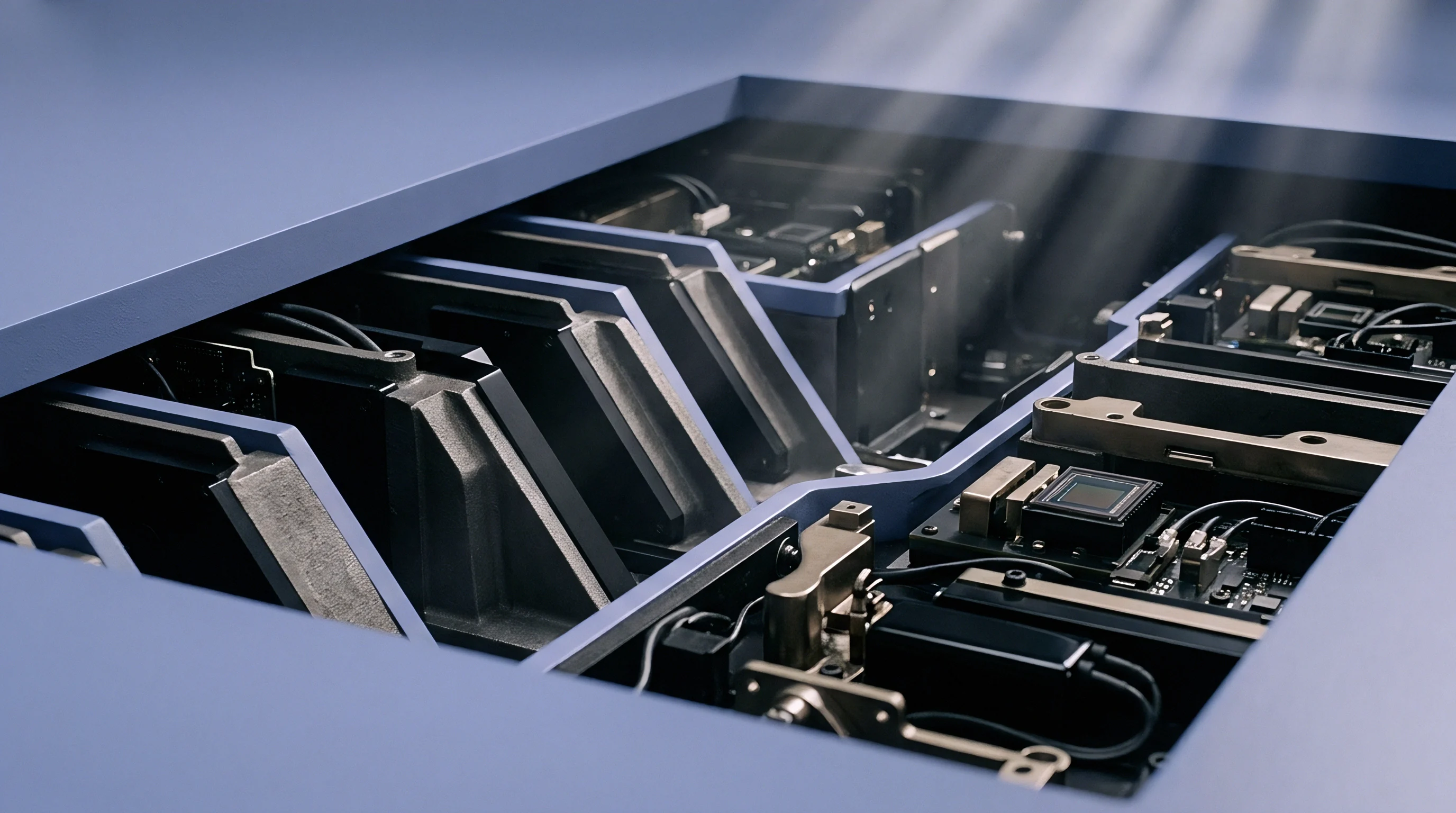
Batch Rework Rates on High Density Arrays
Thermal stress shifts baseline readings. When defective multi-sensor boards enter rework stations, localized infrared desoldering tools apply high thermal energy to extract failed multiplexers or translators. This heating cycle migrates through inner copper ground planes to nearby precision sensors.
Silicon sensing dies subjected to secondary thermal excursions exhibit mechanical stress relaxation across their packaging epoxy, producing permanent output offset shifts.
A precision gyroscope or barometric altimeter can lose its factory calibration after neighboring silicon is desoldered and replaced. The financial cost of re-calibrating an assembled board often exceeds the original manufacturing cost of the entire electronic subassembly. Assembly yield analysis must incorporate these post-rework testing and scrap expenses when evaluating low-cost multiplexers against more distributed hardware architectures.
Routing channels consume inner layers.
Selecting the optimal bus management strategy requires balancing the fixed silicon procurement expense against the lifetime maintenance cost of firmware abstraction layers and manufacturing test yields. Hardware designers evaluate these trade-offs early during schematic capture to avoid redesigning printed circuit boards after mechanical tooling freezes.