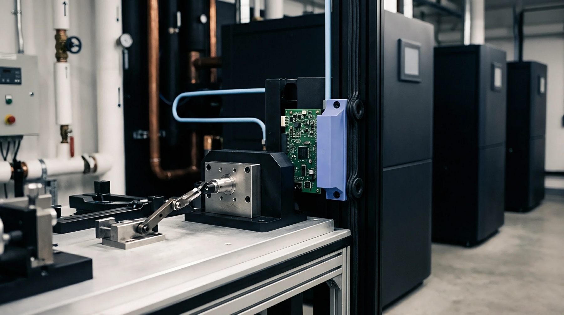
Board Flex Reaching the Die as Offset Error after Assembly
Board flexure transfers shear strain through solder joints into silicon dies, shifting zero-point offsets; isolate footprints using slots or diagonal placement.
Board flexure transfers shear strain through solder joints into silicon dies, shifting zero-point offsets; isolate footprints using slots or diagonal placement.

Compromised MSL 3 packaging instantly voids floor life: quarantine components, verify humidity cards, and require J-STD-033 dry baking before SMT reflow.

Unannounced die shrinks alter internal register maps and bus timing; enforce strict automated register fingerprinting and binding PCN contract terms.
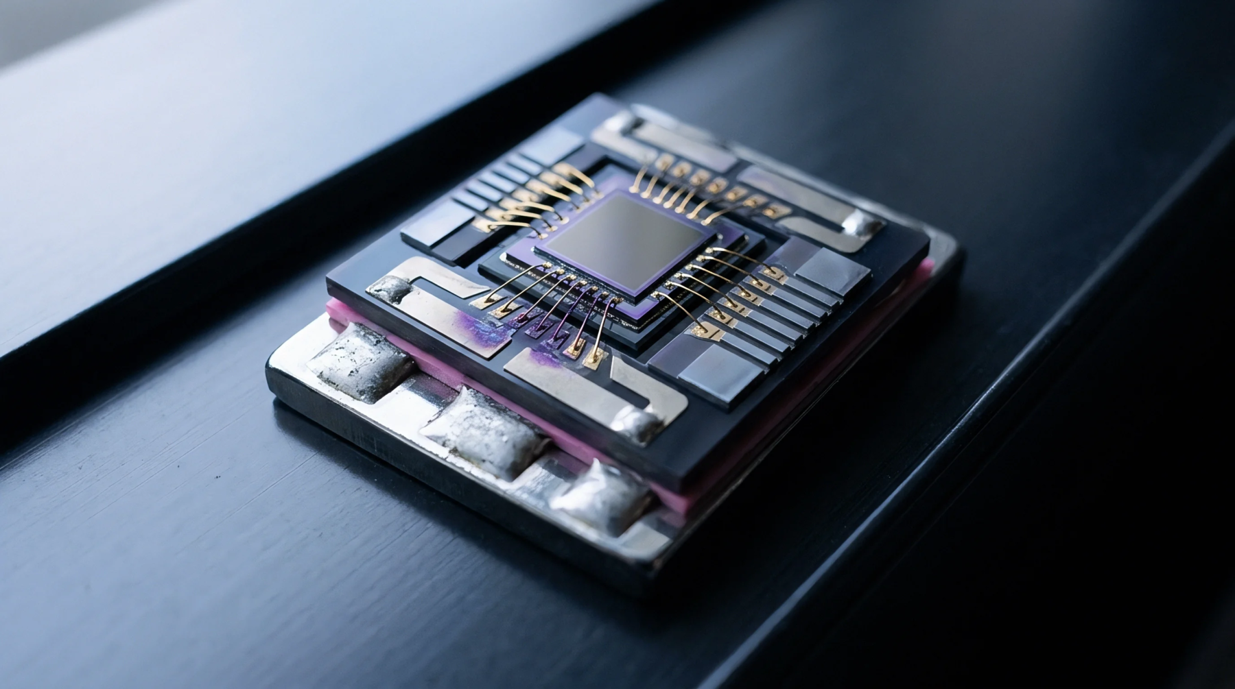
When component vendors end leaded packages, identical active silicon dies often survive in surface-mount forms that demand revised land patterns and thermal layouts.

Epoxy compound moisture absorption generates critical steam pressures during lead-free reflow, demanding strict MSL dry-pack handling to prevent internal delamination.
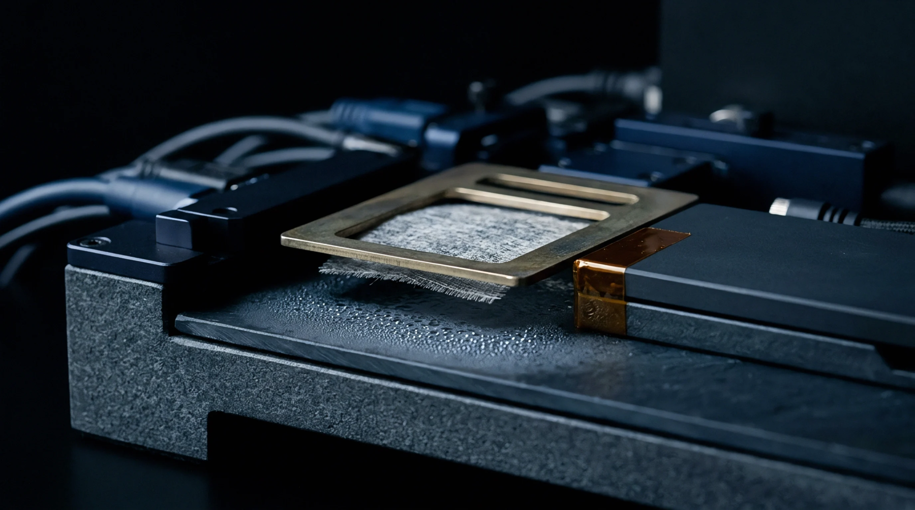
Receiving verification of moisture barrier packaging and strict floor life tracking prevent reflow delamination yield losses in surface mount assembly.

Quantifying supplier liabilities for compromised moisture barrier packaging requires capturing direct component replacement, dry-bake remediation, and SMT line downtime costs under strict quality contract clauses.

Board strain during reflow shifts MEMS digital offsets via CTE mismatch, requiring PCB keep-out zones, low-stress footprints, and 72-hour room-temp stabilization.

Legacy line retrenchment forces silicon die packaging changes that alter kerf tolerances, land patterns, register offsets, and landed unit economics.
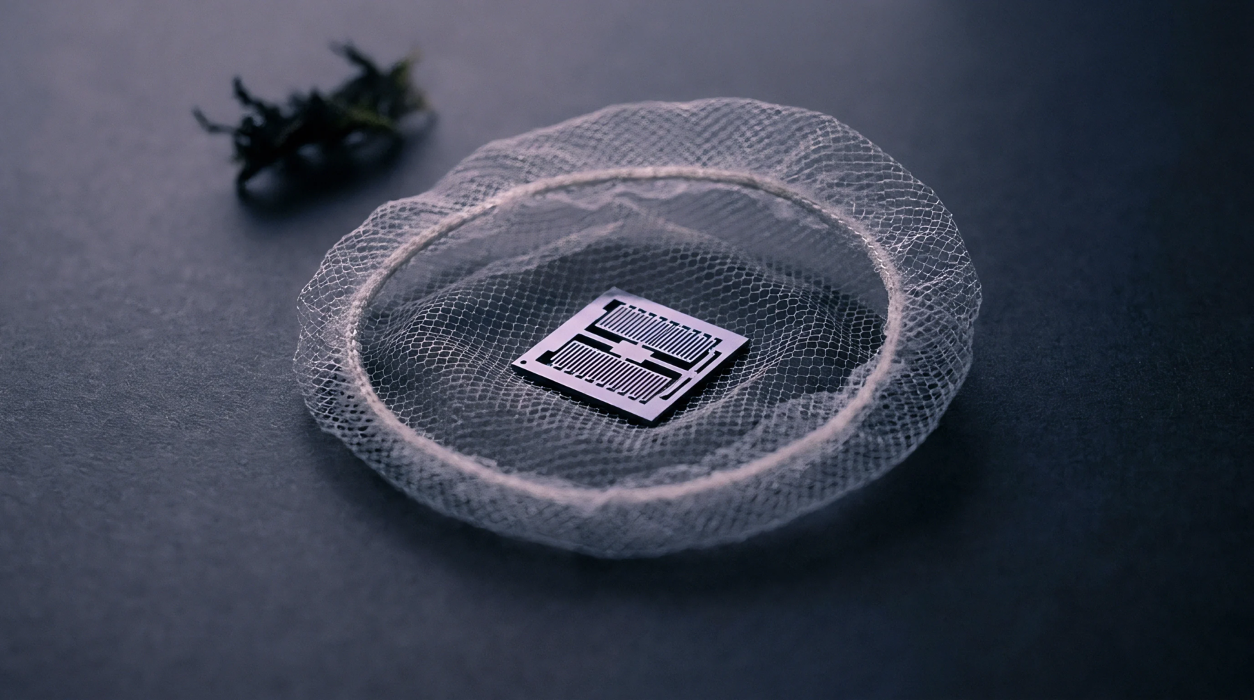
Component reflow popcorning occurs when trapped moisture vaporizes during soldering; acoustic microscopy detects internal delamination via signal phase inversion.

Selecting die packaging forms requires matching land pattern mechanical stress, bus wiring distance, and calibration stability against landed unit economics.

Resolve four-part I2C address collisions using 4-state pin strapping, quad-channel switches, or address translation ICs based on BOM cost and driver complexity.

Driving current from an analog sensor output heats internal silicon sub-circuits, creating thermal gradients that drift the internal voltage reference beyond nominal tolerances.

Sourcing sensor modules eliminates 4 to 12 weeks of driver engineering, flipping break-even economics below 15,000 units despite higher unit BOM prices.

Elevated storage temperatures accelerate moisture diffusion into epoxy molding compounds, raising internal vapor pressure during reflow and driving package failure.

Precision land pattern design balances component manufacturing tolerances against board assembly capability to eliminate thermomechanical stress on silicon die output registers.

External loading on internal voltage references degrades system precision through load droop, substrate thermal gradients, and capacitive loop instability.
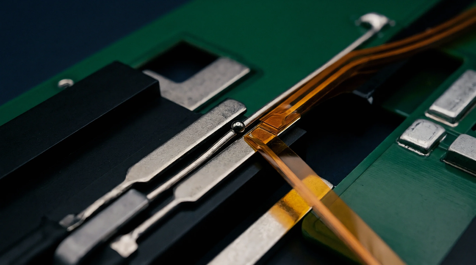
Isothermal component placement, substrate trenching, and balanced copper pours mitigate internal reference voltage drift caused by thermal board stress.

Mechanical board flex induces stress tensor shifts in calibrated silicon die, driving output register offsets beyond rated least significant bit tolerances.

Iso-die package selection dictates backend lead times from 4 to 20 weeks and MOQs up to 50k units, requiring total landed cost models over raw component price.

Verify silicon die revision registers via JTAG or serial readback before firmware boot to catch unannounced stepping changes and protect assembly yield.
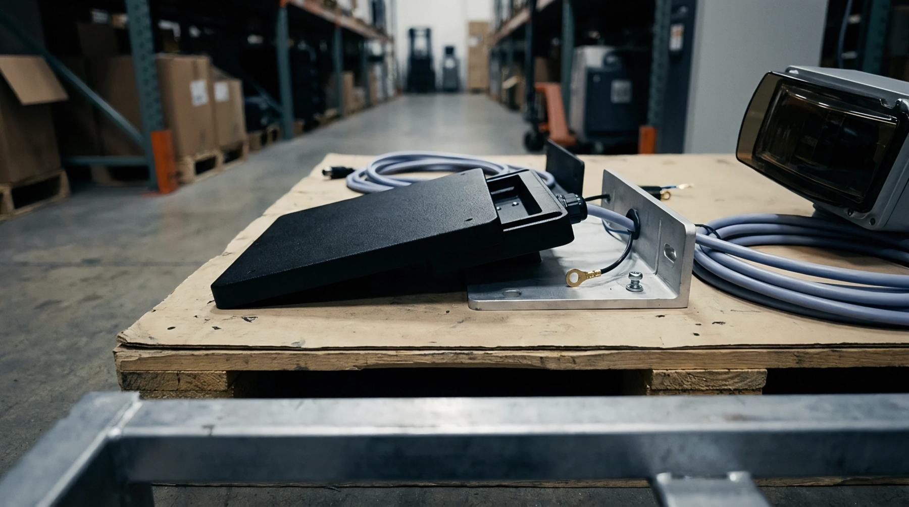
Enforce 18-month EOL notice timelines and silicon-level allocation guarantees to protect sensor supply chains from unannounced component discontinuances.

Sensor package choice dictates board layout tolerances, bus signal integrity, driver firmware complexity, and final landed unit economics across production volumes.

I2C multiplexers resolve address collisions and isolate bus capacitance via software channels, while translators match voltage rails without addressing control.
Epoxy molding compounds absorb moisture according to temperature-dependent diffusion rules, requiring strict MSL floor life management to avoid popcorning during reflow.

Asymmetric output load dissipation creates substrate thermal gradients across monolithic reference dies, inducing microvolt baseline offsets in precision data converters.

Precision bandgap layout demands common-centroid transistor symmetry, localized thermal guard isolation, and PCB stress slots to achieve sub-5 ppm/°C drift.
Board level thermal gradients shift internal bandgap voltages by inducing transistor temperature differentials and piezoresistive package stress.

Mechanical strain alters piezoresistive die Wheatstone bridge resistance, producing analog offset voltages that propagate through gain stages into digital register counts.

Selecting WLCSP over DFN reduces board footprint by 70 percent but introduces strict HDI stackup costs and SMT process controls required to protect yield.
Expertise is a utility, not a secret. sentiention™ publishes its working knowledge as open reference: intelligence layer covering the materials it sources, the markets it enters, and the reference that serves both.