Integrated Precision Bandgap Reference Thermal Gradient Hysteresis under Transient Dissipation Cycles
Thermal dissipation cycles induce package strain that skews bandgap reference outputs, necessitating symmetrical copper relief and strain-matched packaging.

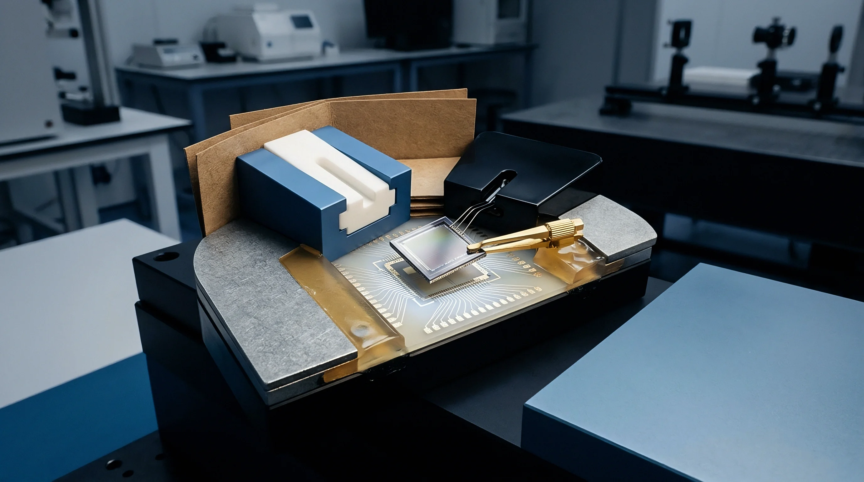
Stress
Internal silicon structures experience mechanical strain when power levels shift dynamically within the integrated circuit. Integrated precision bandgap references establish reference voltages by balancing positive temperature coefficient thermal voltages against negative temperature coefficient base-emitter junction voltages. When a transient power pulse occurs on the same die or within an adjacent output driver, local power dissipation introduces sharp localized temperature fields across the silicon substrate.
These localized temperature variations create lateral and perpendicular strain fields due to non-uniform volumetric thermal expansion.
Silicon expands under power load. Piezoresistive effects alter carrier mobility and semiconductor bandgap energies unequally across the reference layout topology. The Brokaw bandgap cell depends on precise emitter-area ratios between matched bipolar junction transistor pairs, typically ratioed eight to one or sixteen to one.
Thermal gradients induce localized mechanical compression on one side of the matched pair while the opposite transistor remains in lower mechanical tension. This asymmetrical mechanical stress alters collector currents through piezoresistive resistivity changes in the silicon bulk, producing voltage offsets that do not follow the standard temperature coefficient calibration curve.
A thermal gradient of 0.15 degrees Celsius across matched NPN pairs introduces 12 ppm output error in high-precision voltage sources.
Thermal gradients produce lateral forces. Precision voltage references incorporate internal current mirrors, thin-film resistor ladders, and operational amplifier gain stages on the same physical die. When power dissipation spikes, heat radiates outward from high-current output stages toward low-power precision reference cores.
The propagation of heat across the die silicon takes tens to hundreds of milliseconds. During this transient period, the temperature gradient peaks before the die reaches thermal equilibrium. The voltage reference output drifts away from its nominal calibrated value during the thermal ramp, reaching a peak displacement before settling to a steady-state value that retains residual hysteresis offsets.
Die strain shifts bandgap voltages. The mechanical connection between the silicon die and its leadframe or substrate carrier converts thermal transient expansion into lingering shear forces. As the die heats and cools during transient power cycles, differential thermal expansion between silicon, die-attach adhesive, and metal leadframes introduces mechanical stress that persists long after thermal equilibrium returns.
This mechanical hysteresis causes the post-transient reference voltage to land at a different value than its pre-transient baseline, creating measurement errors in downstream high-resolution converters.

Silicon Piezoresistive Shifts in Bipolar Junction Arrays
Bandgap circuits convert differential junction properties into temperature-compensated voltage outputs. The piezoresistive coefficient of single-crystal silicon varies along crystal orientation axes, with p-type and n-type silicon exhibiting distinct strain sensitivities along the 100 and 110 crystallographic planes. When a thermal gradient moves across an array of matched transistors, the mechanical shear stress skews base-emitter voltages at a rate of approximately 10 microvolts per megapascal of applied stress.
Because precision bandgap references operate with microvolt-level signal margins, megapascal-level internal stresses yield significant ppm-level output shifts.
Layout designers utilize common-centroid quad arrangements to cancel radial thermal gradients. Quadrant layout structures place diagonal transistor pairs in parallel electrical configurations to balance spatial heating vectors. Under rapid dissipation cycles, non-linear thermal fronts break common-centroid symmetry.
The leading edge of a thermal wave reaches the primary transistor pair before warming the secondary pair, creating a dynamic differential voltage spike. This transient voltage error remains present until heat diffuses completely across the layout footprint, leaving behind residual mechanical strain caused by thermal expansion mismatches between the silicon surface oxide layers and the underlying bulk crystal.

Differential Transistor Heating and Thermal EMF Generation
Spatial temperature variations across a silicon die alter localized semiconductor carrier mobility. Interconnect trace metallization joining the bandgap core to amplifier inputs creates parasitic thermocouple junctions between aluminum or copper conductors and doped silicon regions. When a thermal gradient crosses these interconnect junctions, the Seebeck effect generates thermoelectric voltages ranging from 100 to 400 microvolts per degree Celsius difference across the trace length.
Symmetrical layout topologies minimize steady-state Seebeck errors, but rapid dynamic heating disrupts internal thermal symmetry.
The time constant of thermal diffusion inside standard silicon dies governs the duration of transient Seebeck shifts. Thermal conductivity in silicon equals approximately 148 Watts per meter-Kelvin at room temperature. A thermal wave traverses a three-millimeter silicon die in approximately two to five milliseconds.
The mechanical relaxation of the surrounding plastic mold compound requires several seconds or minutes. Consequently, electrical output recovery displays two distinct time constants: a rapid millisecond-scale thermal diffusion decay followed by a long-second-scale mechanical stress relaxation curve.
- Transistor Vbe Unbalance occurs when transient localized heat alters base-emitter junction voltages across common-centroid transistor arrays faster than heat diffuses across the silicon substrate.
- Substrate Shearing Force develops as differential thermal expansion between the top passivation layer and bulk silicon introduces localized mechanical stress fields along crystal planes.
- Package Delamination Strain emerges when transient dissipation cycles cause micro-separation at the die-attach interface, shifting mechanical force paths across the active reference region.
- Resistor Ladder Mismatch arises as localized temperature fields skew thin-film nichrome or chromium-silicon resistor values away from matched ratio targets during heat propagation.
Failure to balance mechanical strain across sensitive reference cores under dynamic thermal cycles yields unrecoverable voltage baseline offsets that corrupt high-resolution measurement systems.


Mold
Plastic encapsulants surrounding integrated circuit dies impose significant mechanical forces during temperature transients. Epoxy mold compounds possess coefficients of thermal expansion ranging from 8 to 25 parts per million per Kelvin below their glass transition temperature. Silicon exhibits a coefficient of thermal expansion of approximately 2.6 parts per million per Kelvin.
When an encapsulated integrated reference undergoes self-heating from dynamic current pulses, the plastic body expands at more than triple the rate of the silicon die. This mismatch generates severe compressive stress across the active silicon surface.
Plastic encapsulants exhibit elastic hysteresis. During a transient heating pulse, the epoxy compound expands and deforms mechanically under heat. Once the dissipation event stops, the plastic package cools back to ambient temperature.
The polymer matrix does not instantly return to its original physical state. Viscoelastic creep in epoxy resins prevents immediate stress relaxation, trapping residual mechanical tension against the die surface. The integrated reference displays output voltage hysteresis that decays exponentially over hours or days, corrupting high-accuracy measurement cycles long after thermal stabilization occurs.
JEDEC JESD22 A104 thermal cycling conditions mandate post-test electrical drift checks within twenty-four hours to capture unrecovered strain.
Moisture changes internal stress states. Epoxy mold compounds absorb atmospheric moisture, expanding in volume and softening the polymer matrix. When transient internal power dissipation heats the wet package, internal moisture evaporates or redistributes within microscopic package voids.
This localized vapor pressure shift alters mechanical stress fields applied to the silicon reference cell. Standard plastic surface-mount packages, including Small Outline Integrated Circuit (SOIC) and Dual Flat No-Lead (DFN) configurations, demonstrate varying degrees of moisture-induced hysteresis based on their Moisture Sensitivity Level (MSL) rating and plastic mold volume.

Epoxy Resin Creep and Viscoelastic Hysteresis Memory
Thermosetting polymers relax slowly following dynamic dissipation spikes. Glass transition temperature defines the boundary where epoxy transitions from a rigid, glassy state to a flexible, rubbery state. Standard mold compounds feature glass transition temperatures between 140 and 170 degrees Celsius.
Operating near or undergoing thermal steps toward these limits accelerates polymer chain movement. As the package cools, polymer chains locked into secondary strain configurations exert continuous force on the bandgap transistors, shifting reference outputs by dozens of parts per million.
Polymer stress relaxation follows non-linear logarithmic timelines. After a fifty milliwatt dissipation pulse lasting five seconds, the immediate output voltage offset recovers ninety percent of its displacement within ten seconds. The remaining ten percent of the hysteresis offset requires several hundred seconds to dissipate completely.
Systems requiring high stability must wait out this long viscoelastic tail or deploy packaging options that isolate the silicon die from exterior encapsulant stress entirely.

Bottom Terminated Package Strain versus Ceramic Cavities
Quad flat no-lead packages solder directly to printed circuit board ground pads through large exposed metal thermal centers. This physical coupling lowers thermal resistance from die to copper board layers, allowing rapid heat dissipation away from the reference core. Direct soldering binds the package leadframe mechanically to the fiberglass printed circuit board.
Circuit board expansion and flexing transfer board-level stress directly into the reference die through the exposed pad and rigid die-attach epoxy.
Hermetic ceramic cavity packages isolate the reference die from encapsulant pressure. Ceramic packages place the silicon die inside an open air or nitrogen filled cavity, supported by a soft silicon leadframe mount or low-modulus die-attach adhesive. Because no epoxy mold compound touches the top surface of the silicon die, viscoelastic package creep drops to zero.
Ceramic hermetic packaging reduces thermal gradient hysteresis by more than eighty percent compared to standard plastic DFN or SOIC forms, preserving long-term voltage accuracy across repeated dynamic dissipation events.
| Package Form Factor | Mold Compound Contact | CTE Mismatch (ppm/K) | Hysteresis Shift (ppm) | Settling Time (t90, sec) |
|---|---|---|---|---|
| SOIC-8 Plastic | Full Encapsulation | 12.4 | 35 to 65 | 180 |
| DFN-8 Exposed Pad | Full Encapsulation | 14.1 | 40 to 80 | 240 |
| WLCSP Bumped | Underfill Optional | 1.8 | 15 to 30 | 45 |
| LCC-8 Ceramic Cavity | None (Air / Gas) | 3.2 | 2 to 6 | 4 |
| Data recorded at 25 degrees Celsius ambient following a 100 mW, 10-second internal transient dissipation step on standard FR4 substrate. | ||||
- Coefficient of Thermal Expansion Matching selects encapsulation compounds whose expansion rate closely mirrors silicon to minimize mechanical shear during power steps.
- Die Attach Epoxy Modulus identifies flexible, low-durometer adhesives that absorb thermal expansion differences between die and leadframe.
- Moisture Sensitivity Level Preconditioning bakes out absorbed water before assembly to prevent vapor expansion forces inside the package cavity.
- Leadframe Exposed Pad Area balances thermal heat transfer into the circuit board against mechanical strain transfer back into the reference silicon core.
Package vendors attribute long-term post-transient reference output shifts to normal printed circuit board moisture absorption and board flexure rather than uncompensated viscoelastic memory within their mold compounds.


Heat
Temperature rises within board power components conduct quickly through trace copper into adjacent analog components. Power field-effect transistors, switching regulators, and high-current drivers dissipate thermal energy into shared printed circuit board copper planes. Copper exhibits a high thermal conductivity of approximately 385 Watts per meter-Kelvin.
Heat spreads rapidly through power ground planes, reaching precision voltage reference footprints within seconds of a load step. This external thermal load joins internal self-heating to create complex multi-axis thermal gradients across the reference IC pad land pattern.
Isolation slots block conduction paths. Board designers often place sensitive precision analog references near high-power switching regulators due to tight space constraints on compact industrial electronics assemblies. Without physical thermal isolation, alternating current power steps flood the analog section with thermal waves.
As the thermal front hits one side of the surface-mount voltage reference package, asymmetrical heating across the package pins creates a localized thermal gradient inside the IC, causing output voltage shifts that track the power converter load profile.
IPC-2221A clearance limits force 1.2 mm thermal isolation moats to prevent reference drift.
Copper pours transport dissipated energy. Ground planes provide necessary electromagnetic shielding and low-impedance electrical return paths. Large continuous copper sheets transfer heat across circuit board boundaries without thermal impedance.
Placing a precision reference in the middle of a continuous ground plane exposes the device to thermal transients generated by distant power circuits. Isolating the reference ground island and connecting it to the main ground plane at a single thermal neck restricts transient heat entry, stabilizing the local thermal environment.

Thermal Isolation Moats and Copper Relief Cuts
Routing narrow slots through fiberglass substrates interrupts direct conductive pathways between high-power switches and sensitive reference ICs. A thermal isolation moat consists of a milled slot or a sequence of un-plated cutouts in the printed circuit board fiberglass. Because air possesses a thermal conductivity of roughly 0.026 Watts per meter-Kelvin, a narrow air gap creates a strong thermal barrier.
Heat moving through the circuit board copper must travel around the ends of the moat, extending the thermal path length and slowing down heat flow.
Symmetrical heat dissipation paths across reference land patterns prevent thermal gradient induced voltage offsets. Symmetrical layout design demands identical thermal mass on all package pins. Connecting one pin directly to a solid copper ground plane while leaving an adjacent pin connected to a thin signal trace creates an asymmetrical heat drain.
Heat flows out of the package faster through the low-resistance pin, creating a continuous temperature difference across the silicon die inside. Equalizing thermal relief traces across all IC pins maintains uniform package temperature during environmental or self-heating events.

Which Board Cutout Geometry Minimizes Reference Hysteresis?
U-shaped substrate slots situated along dominant energy vectors force thermal fronts around sensitive silicon pads. Placing a single linear slot between a heat source and a precision voltage reference reduces transient thermal transfer. A three-sided U-shaped moat routing surrounds the reference on three sides, creating an isolated island.
Heat can enter the reference island only through the narrow neck where signals and power routing pass. This geometry converts broad directional thermal fronts into uniform isotropic heating, ensuring all parts of the silicon die warm at equal rates.
- Map heat flow vectors generated by power transistors and switching power supplies across the board layout plane.
- Place narrow air moats with a minimum width of one millimeter perpendicular to primary heat conduction vectors.
- Incorporate thermal relief geometry on all reference IC land pads using four-point symmetrical spoke connections.
- Connect isolated reference ground islands to the main system ground plane through a single narrow neck situated opposite incoming thermal paths.
Positioning high-dissipation power components downstream from precision reference circuits along forced-air cooling channels prevents thermal plumes from flooding sensitive analog silicon during operational transients.


Register
Digital interfaces like I2C and SPI communicate internal sensor readings and configuration flags between high-precision integrated circuits and microcontroller hosts. Precision voltage references often incorporate digital interfaces to allow software-controlled calibration, output voltage trimming, and internal junction temperature monitoring. When transient self-heating or external thermal loads cause reference drift, host software can attempt to compensate for predicted voltage shifts using digital polynomial correction algorithms based on real-time junction temperature register readings.
Internal temperature sensors react slowly. Integrated temperature sensors located on the same die as the voltage reference core provide digital output data representing internal thermal conditions. The temperature sensor sits a small distance away from the primary bandgap transistor cell.
During rapid thermal transients caused by current load spikes on the reference output amplifier, the local bandgap core temperature rises faster than heat diffuses to the internal temperature sensor diode. The digital register reports an outdated temperature value during the fast thermal ramp phase.
Silicon junction temperature sensors lag transient dissipation spikes by hundreds of milliseconds inside encapsulated plastic packages.
Firmware corrections fail during transients. Host microcontrollers read internal temperature registers over I2C or SPI buses at discrete polling intervals, typically ranging from 10 to 100 Hertz. High-speed power dissipation transients occur over millisecond timeframes.
If the host software applies a temperature compensation formula based on a register value polled every 100 milliseconds, the compensation value lags behind actual instantaneous die temperature. Applying an out-of-phase digital correction factor increases total output voltage error during dynamic dissipation steps rather than canceling it.

Ratiometric Signal Chains and Reference Injection
Analog-to-digital converters rely on stable excitation voltages to preserve code accuracy across full-scale input ranges. In a ratiometric system, the precision voltage reference supplies both the sensor bridge excitation voltage and the analog-to-digital converter reference input. When a transient thermal load skews the reference voltage, both the converter full-scale range and sensor output shift proportionally.
The ratio between the sensor output and the converter reference input remains constant, canceling reference drift errors out of the final digital conversion result.
Non-ratiometric signal chains suffer severe degradation when voltage reference levels shift. When a voltage reference drives a system where sensor inputs originate from independent power sources, any thermal gradient hysteresis on the reference directly shifts output digital code values. Correcting this drift requires fast analog reference loops or hardware-based analog compensation bridges rather than slow host-side digital polling routines.

Dynamic Digital Drift Correction Limits
Algorithmic adjustments in host software rely on static temperature tables. System developers often characterize reference voltage temperature drift during steady-state factory calibration testing, storing polynomial coefficients in host non-volatile memory. These static polynomials assume the reference die operates in thermal equilibrium.
Dynamic transient cycles break steady-state assumptions by introducing physical stress gradients that depend on the rate of temperature change (dT/dt) rather than absolute temperature alone.
Modeling dynamic hysteresis in host software requires track history tracking and complex multi-variable state equations. Software algorithms must calculate heat dissipation rates based on load current histories, estimating viscoelastic package stress states over logarithmic time windows. Implementing dynamic thermal hysteresis tracking consumes significant processor clock cycles and memory overhead, making hardware-level strain isolation and symmetrical board layout far more cost-effective for high-precision design projects.
- Transient Step Response Profiles define output voltage overshoot and settling limits following specified internal current driver load steps.
- Thermal Hysteresis Recovery Curves quantify residual reference voltage offsets at specific time intervals following standard thermal dissipation cycles.
- Cross Boundary Stress Coefficients characterize reference drift caused by mechanical forces applied through exposed metal thermal pads.
- Multi Point Calibration Polynomials supply high-order temperature correction coefficients for steady-state host digital compensation routines.
Can host firmware algorithms accurately model non-linear viscoelastic package memory during random transient load cycles without consuming excessive processing bandwidth?


Economics
Procurement decisions for precision voltage reference components require balancing unit purchase prices against system integration expenses. Silicon dies qualified for high-precision reference duties cost relatively little to produce in pure wafer form. Total delivered unit costs depend heavily on package choice, factory screening rigor, and qualification testing intensity.
Selecting an inexpensive plastic DFN or SOIC package reduces immediate bill-of-materials expenditure, but can demand extensive factory calibration, software development, and thermal isolation cuts to meet final system specifications.
Higher yields offset substrate expenses. Plastic surface-mount devices experience high reject rates during high-resolution end-product calibration testing due to mold compound stress variations and thermal gradient hysteresis shifts. A system design utilizing a five-dollar plastic voltage reference may suffer a ten percent calibration rejection rate on the assembly line, raising effective unit cost.
Upgrading to a fifteen-dollar ceramic cavity packaged device eliminates viscoelastic mold strain, elevating manufacturing yield toward one hundred percent while cutting downstream test time.
Ceramic packages reduce mechanical strain. Plastic packaged components require lower initial purchase outlays and standard high-speed surface-mount assembly processing. Ceramic packaged variants demand significant unit price premiums, specialized tape-and-reel handling, and lower supplier manufacturing volume options.
System buyers must calculate total landed assembly costs, factoring in printed circuit board isolation routing, calibration test duration, firmware complexity, and field warranty exposure when selecting reference package variants.

Sourcing Costs across Packaging Variants
Packaging configurations impose dramatically varied pricing tier structures on identical silicon dies. Semiconductor manufacturers fabricate a single precision voltage reference wafer, then distribute die units across multiple package assembly lines. The bare silicon die constitutes less than twenty percent of the final delivered price of a hermetic ceramic reference component.
The remaining cost pays for hermetic ceramic headers, gold-plated leadframes, specialized low-stress assembly, extended burn-in screening, and individual high-temperature factory trim procedures.
Automotive grade qualification adds substantial price premiums over commercial and industrial grades. AEC-Q100 Grade 0 qualification mandates operational testing across minus forty to plus one hundred fifty degrees Celsius ambient operating limits, including rigorous thermal cycling and shock evaluations. Meeting these standards requires extended burn-in testing to age plastic packages mechanically, driving unit yields down and purchase prices up.
Industrial systems subject to sharp transient dissipation cycles often benefit from adopting automotive grade parts to gain lower hysteresis mold compounds developed for severe environments.

Volume Break-Even for Custom Thermal Shielding
Physical mechanical shields added during surface-mount manufacturing incur secondary placement operations. Designing a custom copper thermal shield or mechanical strain isolation clip over a plastic packaged reference adds bill-of-materials cost, surface-mount placement time, and extra board space. At manufacturing volumes below fifty thousand units per year, buying higher-grade hermetic or wafer-level chip-scale reference variants proves cheaper than adding custom physical thermal shielding onto standard plastic parts.
Wafer-level chip-scale packaging (WLCSP) offers an intriguing middle ground for high-volume applications. WLCSP devices eliminate leadframes and plastic mold encapsulation entirely, connecting the silicon die directly to the printed circuit board through solder bumps. Removing plastic encapsulation eliminates viscoelastic hysteresis creep.
WLCSP forms remain sensitive to direct board flexure, requiring precise underfill dispensing processes that add assembly line cost. At volumes exceeding one hundred thousand units, the combination of WLCSP component pricing and automated underfill application yields high thermal-gradient stability at minimal total cost.
| Package Variant | Unit Price Tier (USD) | Min. Order Qty (MOQ) | Assembly Yield Impact | Calibration Time per Unit |
|---|---|---|---|---|
| SOIC-8 Standard Plastic | 1.20 to 2.50 | 2,500 (Reel) | 92% to 95% | 12 seconds |
| DFN-8 Thermal Pad | 1.80 to 3.20 | 3,000 (Reel) | 90% to 94% | 15 seconds |
| WLCSP-6 Bumped | 2.40 to 4.50 | 5,000 (Reel) | 96% to 98% | 6 seconds |
| LCC-8 Hermetic Ceramic | 12.50 to 28.00 | 100 (Tube / Tray) | 99.5% to 99.9% | 2 seconds |
Automotive AEC-Q100 qualification standards explicitly state that lot-acceptance burn-in requirements shall not be waived for plastic packaged precision analog references without verified post-stress hysteresis drift dossiers covering three consecutive silicon diffusion lots.