
Surface Mount Footprint Tolerances for Pressure and Inertial Transducers
Holding land pattern pad widths to plus or minus twenty-five micrometers isolates MEMS sensing elements from board warpage and eliminates post-reflow zero drift.
Holding land pattern pad widths to plus or minus twenty-five micrometers isolates MEMS sensing elements from board warpage and eliminates post-reflow zero drift.

Dynamic firmware compensation for solder strain drift demands strictly bounded tracking windows to prevent ADC resolution loss and false baseline nulling.

Calculate bus parasitic limits by summing pin, pad, and trace capacitance against standard rise-time formulas to fix pull-up values before board layout freezes.
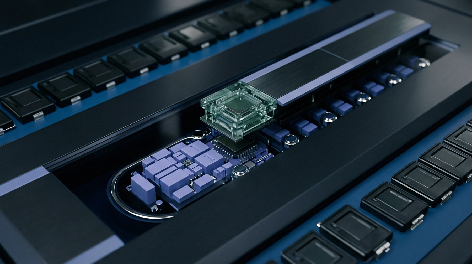
Land pattern calibration requires balancing IPC-7351 solder fillet dimensions against fabricator tolerance limits to maximize assembly yield and high-speed signal integrity.
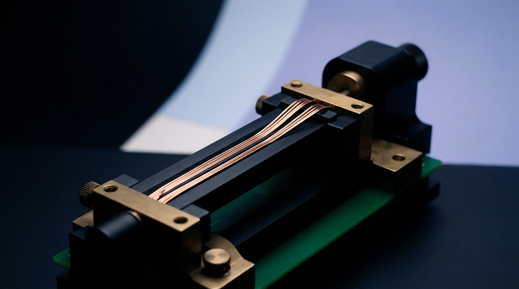
Bismuth segregation at copper intermetallic boundaries induces brittle cleavage under rapid drop shock, demanding microalloyed dopants to preserve high-velocity toughness.

Finite element modeling of underfill viscoelastic creep enables precise prediction of die stress relaxation and dynamic digital offset drift in encapsulated sensors.
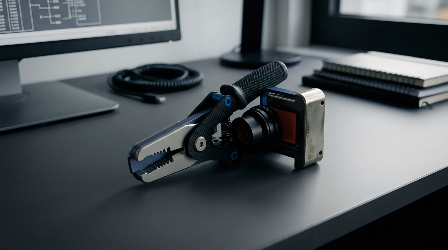
Asymmetric epoxy swelling induces die bending stress and digital zero-point calibration drift, requiring package isolation and specific land pattern geometries.
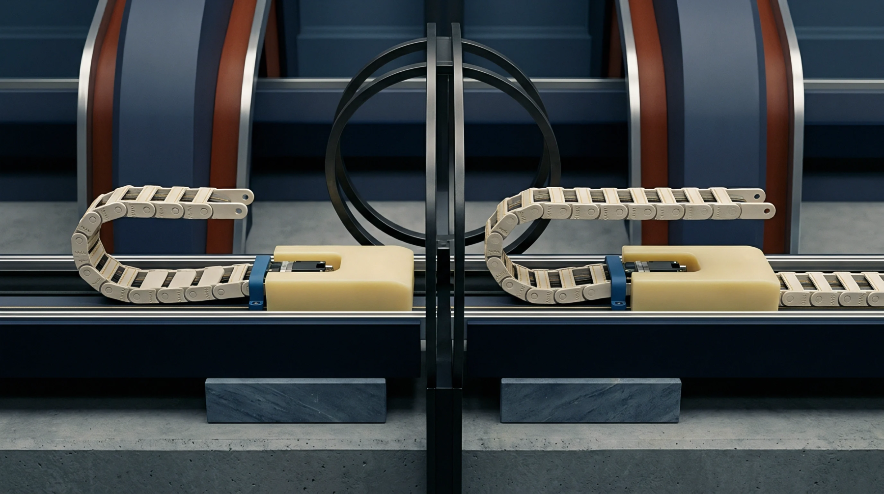
Board flexure fatigue failure is mitigated by limiting strain energy density accumulation through NSMD pad geometry, SAC105 alloy selection, or corner underfill.

Analytical strain attenuation models quantify flexural stress transfer through solder lands, enabling optimized patterns that prevent sensor drift and joint fatigue.
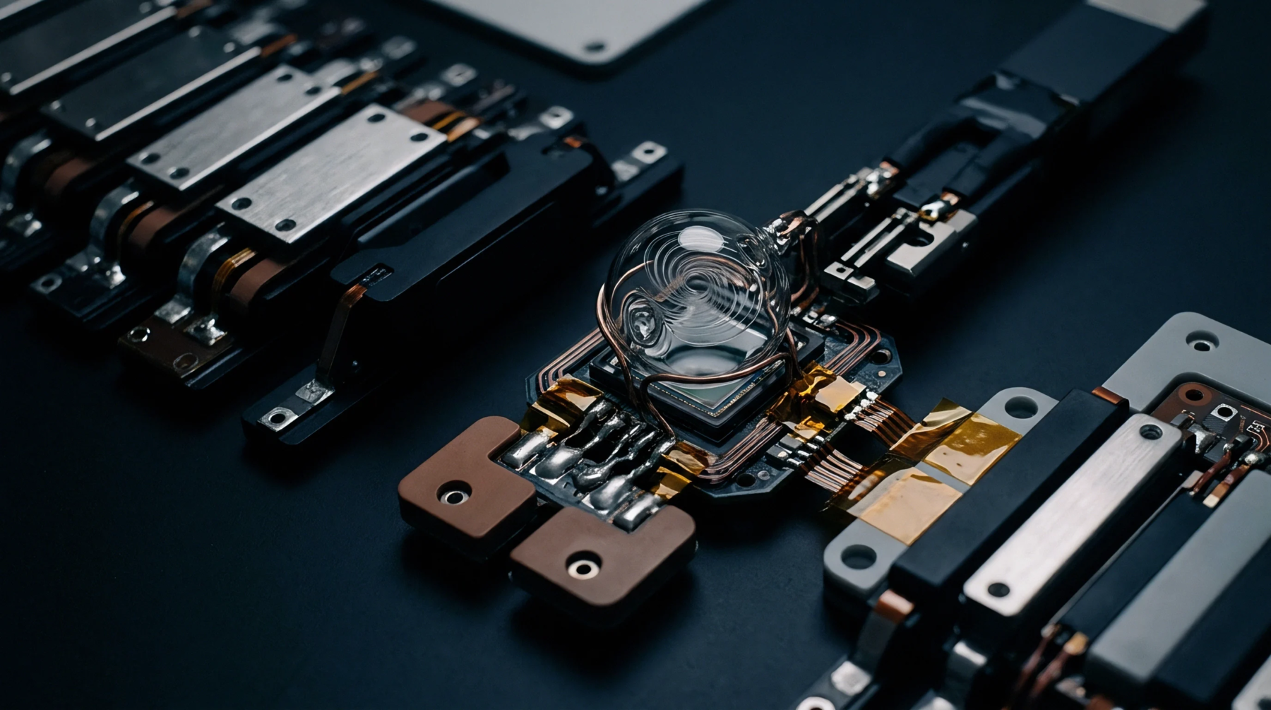
Interfacial shear lag concentrates thermal mismatch forces at package corners, requiring precise standoff height and pad geometry control to prevent joint fatigue.

Calibrated Anand viscoplastic modeling predicts solder joint thermal fatigue life by coupling rate-dependent strain energy accumulation to board-level packaging geometry.

Wafer-level package shear mechanics rely on ball standoff height, pad geometry, and underfill to mitigate thermal expansion mismatch across solder joints.

Tensorial stress analysis maps dynamic reflow shear and peel forces across package substrates to prevent non-wet opens and mitigate board-level solder cracking.

Dynamic asymmetric thermal cycles induce unrecoverable solder creep that relaxes packaging stresses, shifting precision sensor baselines over operating time.
Minimizing reference drift requires non-solder-mask-defined pads, compliant gull-wing packages, and perimeter routed slots to isolate circuit board strain.
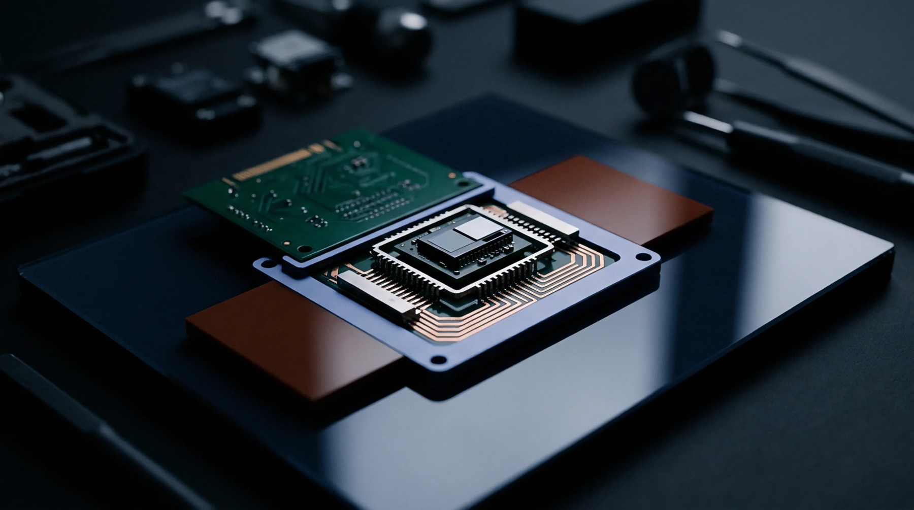
Wafer-level package parasitic inductance variance shifts serial channel return loss and eye margins, requiring strict standoff height controls during assembly.

Post-reflow zero-point drift stems from package-to-board thermal expansion mismatch, demanding compliant leads or post-assembly firmware calibration.
Thermal expansion mismatch in fine-pitch packages concentrates shear strain in outer joints, demanding matched underfill and strict standoff control to survive.

Lead-free solder creep relaxes reflow shear stress at ambient storage temperatures, tilting MEMS anchors and driving uncalibrated zero drift over time.

Control surface-mount sensor zero offset by isolating board flex with PCB relief slots, selecting low-modulus die attach packages, and balancing solder volume.
Cascade enable logic eliminates individual chip-select routing across dense sensor arrays by propagating a single hardware token down a shared serial bus.

Extract leadless package parasitics using 3D field solvers and route unbroken ground returns under thermal pads to suppress inductive ground bounce.
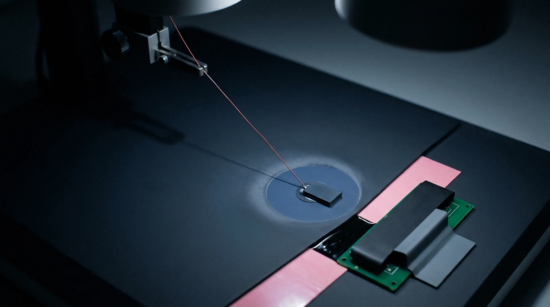
PCB deformation transfers mechanical strain through solder joints into surface-mount sensor dies, causing severe zero drift that requires package isolation or layout slots.

Iso-die package selection dictates backend lead times from 4 to 20 weeks and MOQs up to 50k units, requiring total landed cost models over raw component price.
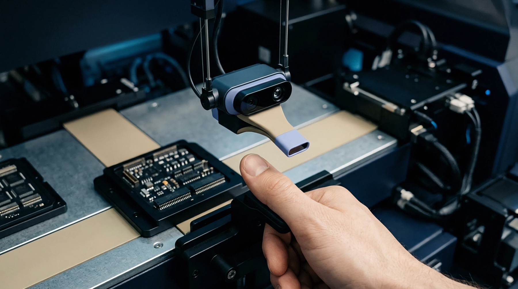
Precision land pattern design balances component manufacturing tolerances against board assembly capability to eliminate thermomechanical stress on silicon die output registers.
Expertise is a utility, not a secret. sentiention™ publishes its working knowledge as open reference: intelligence layer covering the materials it sources, the markets it enters, and the reference that serves both.