
Evaluating SMT Yield Loss and Calibration Cost in Discrete Transducer Assembly
Discrete transducer SMT yield loss and calibration costs depend on pad symmetry, post-reflow strain aging, and test cell chamber dwell times.
Discrete transducer SMT yield loss and calibration costs depend on pad symmetry, post-reflow strain aging, and test cell chamber dwell times.

Elastomer creep alters baseline compressive stress on MEMS packages, causing long term zero drift that requires digital firmware offset compensation.
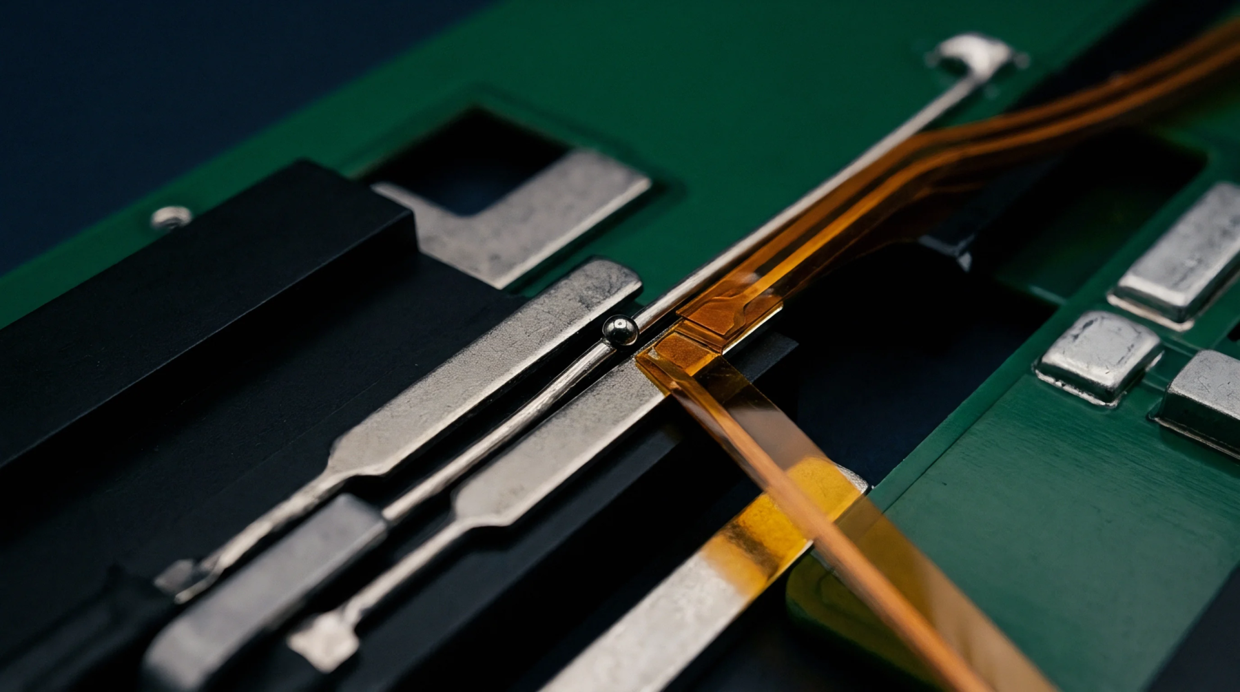
Milled PCB isolation slots and controlled solder standoff heights decouple surface mount pressure sensors from assembly flexure and thermal board strain.

Matrix compensation algorithms correct non-linear thermal piezoresistive drift by mapping raw bridge and temperature counts through fixed-point polynomial surfaces.
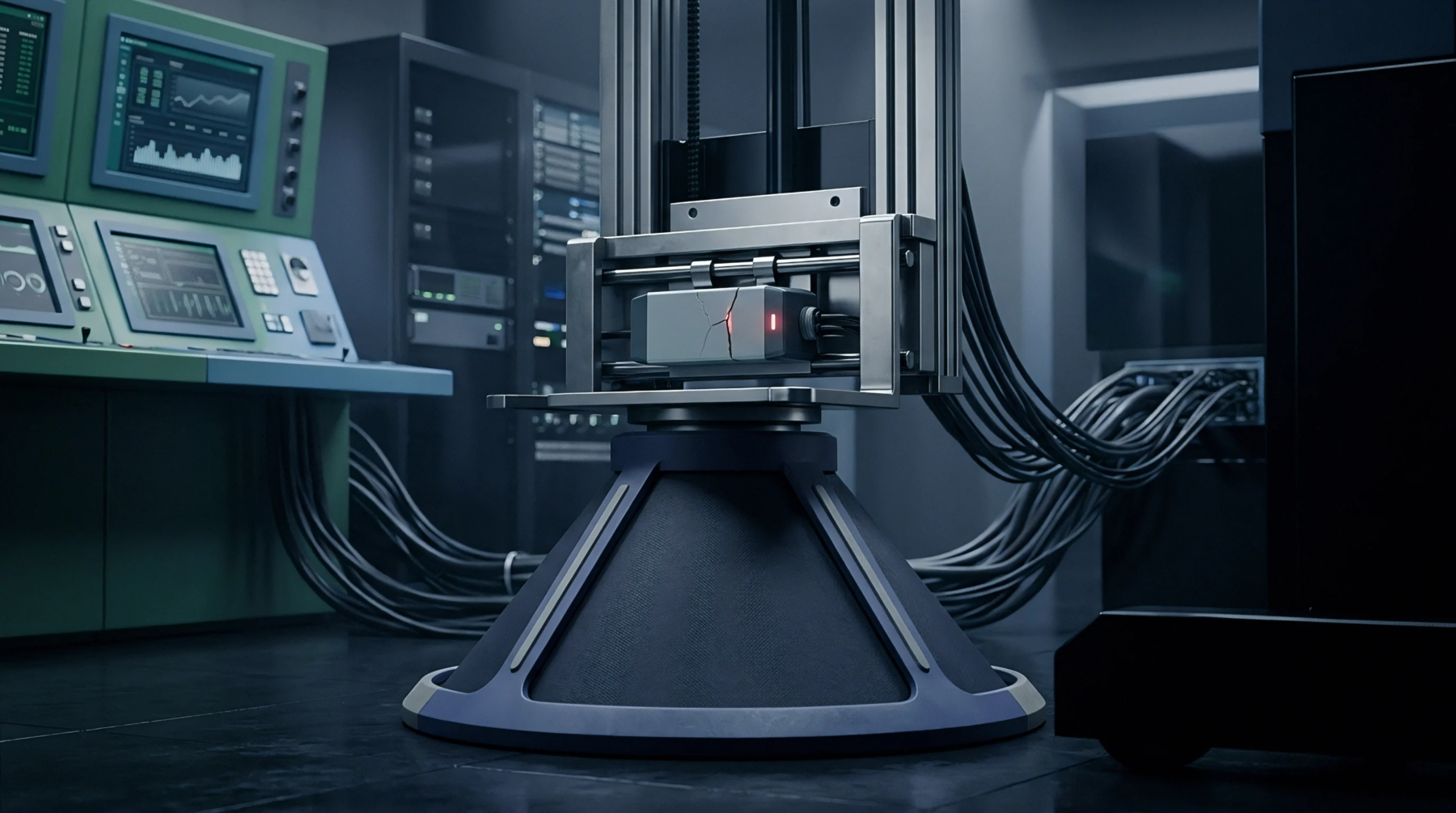
Dynamic asymmetric board strain couples into silicon piezoresistors via solder joints, causing uncompensated baseline drift mitigated by PCB isolation slots.
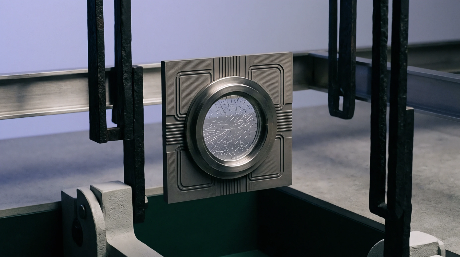
Interfacial hygroscopic swelling stress arises from differential moisture expansion, compounding thermal mismatch and driving package delamination during reflow.

Component obsolescence decisions require balancing upfront board redesign NRE against multi-year nitrogen storage capital tie-up and solderability decay risks.

High modulus mold compounds induce dynamic calibration shifts in sensors; sourcing specs must cap flexural modulus below 18 GPa to protect signal accuracy.
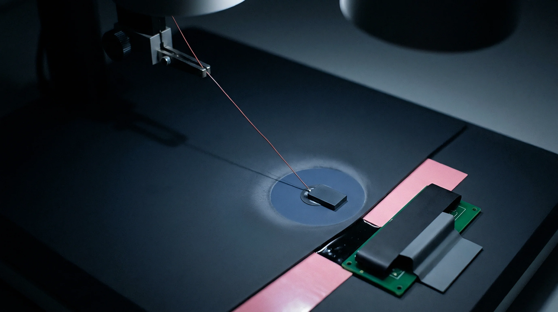
PCB deformation transfers mechanical strain through solder joints into surface-mount sensor dies, causing severe zero drift that requires package isolation or layout slots.

External analog load currents extract direct current and charge pulses from internal bandgap reference nodes, inducing static droop and transient conversion errors.
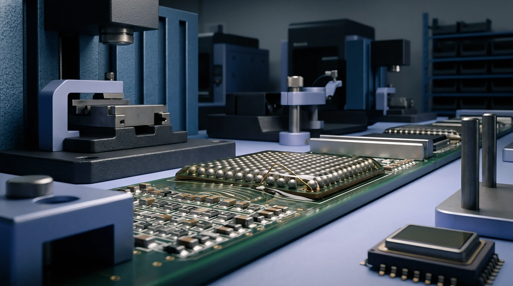
Calculated land pattern dimensions matching IPC-7351 guidelines balance solder fillet volume and placement tolerance to prevent joint stress and yield loss.

Discrete SMD sensors break even over integrated serial modules above fifty thousand units when assembly yields exceed ninety nine percent.

Early silicon steppings lock up I2C clock stretching during ACK phases, requiring firmware timeouts and board RC tuning across packaging revisions.

Board level thermal gradients shift internal bandgap voltages by inducing transistor temperature differentials and piezoresistive package stress.
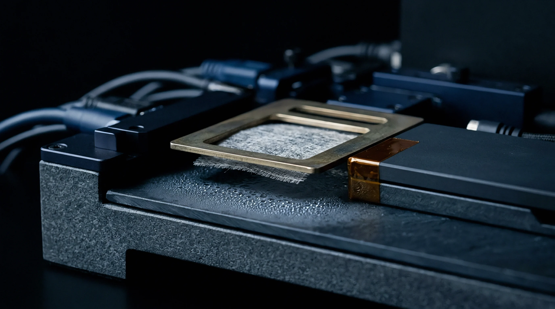
Receiving verification of moisture barrier packaging and strict floor life tracking prevent reflow delamination yield losses in surface mount assembly.
Expertise is a utility, not a secret. sentiention™ publishes its working knowledge as open reference: intelligence layer covering the materials it sources, the markets it enters, and the reference that serves both.