Substrate Warpage Effects on Digital Pressure Sensor Analog Front End Registers
Substrate warpage injects mechanical strain directly into the sensing die, shifting analog front-end bridge balance past digital trim limits.


Bow
Reflow soldering subjects a bare land grid array package to differential thermal expansion between the organic circuit board and the silicon element. During solder solidification, the multi-layer printed circuit board contracts at a rate dictated by its resin content, copper balance, and glass weave orientation. The sensor package substrate, often a thin bismaleimide triazine laminate or ceramic base measuring between 0.20 mm and 0.45 mm in thickness, experiences bending moments transferred directly through the solidifying solder joints.
Silicon exhibits high piezoresistive sensitivity. When the supporting substrate bows, mechanical shear and tensile stresses distort the micromachined silicon diaphragm housed within the package cavity.
This mechanical deformation alters the internal electrical balance of the analog front end long before digital communications begin. Piezoresistive pressure sensors employ four doped resistors arranged in a Wheatstone bridge topology across an etched silicon membrane. Any physical package warpage alters the resting resistance of these bridge arms unevenly.
The resulting differential offset voltage propagates directly into the analog-to-digital converter input stages, corrupting the factory-trimmed calibration points recorded in nonvolatile register banks. Assembly thermal profiles dictate warpage. Unchecked substrate curvature shifts digital output registers off their factory baseline by several hundred Pascals, exceeding the allowable tolerance window of precision barometric and altimetric instruments.

Reflow Induced Package Curvature
Thermal gradients during peak solder liquidus drive dynamic out-of-plane displacement across thin sub-millimeter substrates. Package warpage during surface mount reflow typically follows a predictable transition from convex behavior at room temperature to concave behavior at peak temperatures of 245 degrees Celsius to 260 degrees Celsius, returning to an unpredictable warped profile upon cooling. JEDEC JESD22-B112 defines standard methods for evaluating these out-of-plane displacements using shadow moire interferometry.
For a standard 2.0 mm by 2.0 mm by 0.8 mm 8-pin land grid array pressure sensor, dynamic warpage limits must stay below 35 micrometers across the package diagonal to prevent non-coplanar solder bridging. Substrate warpage of 15 micrometers to 25 micrometers induces substantial mechanical curvature across the mounted silicon die.
Die attachments creep over time. When the die attach epoxy cures, it creates an internal shear plane between the silicon die bottom and the package cavity floor. High-modulus conductive adhesives transfer nearly 80 percent of board-level bending directly to the die edges, whereas low-modulus silicone or fluoro-silicone die attach materials absorb a significant portion of this displacement.
When purchasing sensors in mass production, component engineering teams frequently discover that component vendors have substituted die attach formulations between production lots to optimize manufacturing throughput. This unannounced modification alters the mechanical transfer function between the package substrate and the sensing diaphragm, rendering earlier board-level thermal compensation models completely invalid.

Thermoelastic Mismatch across Printed Circuit Assemblies
Differential coefficients of expansion between glass-reinforced FR4 laminates at 14 to 17 parts per million per Kelvin and silicon dies at 2.6 parts per million per Kelvin generate permanent residual tension upon cooling. When a lead-free SAC308 or SAC305 solder joint transitions from liquid to solid phase around 217 degrees Celsius, the entire assembly locks into a zero-strain reference state at an elevated temperature. As the board returns to 25 degrees Celsius ambient, the PCB contracts significantly more than the package substrate, forcing the package into a pronounced convex crown.
Copper balances determine local bending. If the inner copper layers beneath the sensor land pattern contain asymmetric power planes or dense trace routings, the resulting localized thermal contraction introduces asymmetric twisting along the sensor package axes.
The resulting package distortion induces distinct mechanical and electrical failure modes across the internal sensor architecture:
- Asymmetric bridge arm elongation creates a baseline differential voltage that consumes up to 30 percent of the analog front end programmable gain amplifier dynamic range.
- Die metallization layer microcracking produces intermittent contact resistance along aluminum-copper trace routings, generating localized 1/f flicker noise in low-frequency pressure registers.
- Silicon diaphragm stress localization shifts the zero-pressure sensor transfer curve along its pressure axis while simultaneously altering the second-order temperature compensation coefficient.
- Package lid seal delamination compromises hermeticity in absolute reference sensors, allowing ambient moisture to enter the cavity and introduce dielectric drift across capacitive sensing cells.
Uncorrected mechanical warping shifts the zero-pressure baseline across production batches, sending thousands of calibrated assemblies into the scrap bin when downstream sensor data fails final functional testing.


Transmission
Mechanical energy travels from the printed circuit board through the peripheral solder joints into the molded package base. The physical solder joints do not behave merely as electrical contacts; they function as stiff mechanical cantilevers connecting two bodies with disparate thermoelastic properties. In leadless packages such as land grid arrays and quad-flat no-leads formats, standoff heights rarely exceed 30 micrometers to 50 micrometers after reflow.
This minimal vertical clearance leaves virtually no compliant volume to absorb board-level shear strains. Board flex ruptures package seals. The strain energy flows unimpeded through the copper landing pads, through the solder alloy microstructures, and into the package redistribution layer.
A 50-micrometer deflection across an unrouted FR4 test coupon creates an 85-Pascal baseline shift in a rigid-epoxy land grid array pressure sensor at 25 degrees Celsius.
The physical path continues through the substrate core into the adhesive bond line beneath the micro-electro-mechanical systems sensor die. Solder joints freeze incoming displacement. Die attachment adhesives characterized by high glass transition temperatures freeze into rigid glass-like states below 120 degrees Celsius, transmitting approximately 70 to 85 percent of incoming substrate shear strain into the silicon die bulk.
Low glass transition silicone adhesives, while decoupling the die mechanically, introduce long-term creep and hysteresis under sustained pressure and temperature cycling. Sensor diaphragms measure total deflection. When the die experiences uneven biaxial tension, the micromachined membrane deflects independently of external atmospheric pressure, forcing the analog front end to digitize phantom physical displacement.

Solder Ball Shear and Die Deflection
Localized plastic flow inside tin-silver-copper solder joints acts as the initial mechanical conduit between the circuit laminate and the sensor housing. Solder joint fatigue and creep relaxation occur continuously at room temperature, meaning that warpage stresses do not remain static after assembly. During the first 72 to 168 hours post-reflow, lead-free solder alloys undergo room-temperature grain coarsening and dislocation rearrangement.
This metallurgical relaxation causes the mechanical stress field on the sensor die to drift, resulting in continuous baseline register changes even when the device rests in a completely sealed, temperature-stabilized pressure vessel. Solder creep shifts calibration data.
Different packaging architectures attenuate or amplify this mechanical strain transmission depending on internal construction. Optical telescope mirror mounts employ kinematic flexures to isolate precision glass from mechanical chassis distortion, and an analogous isolation must exist within sensor packaging. Molded plastic packages with overmolded epoxy caps experience severe thermal stress due to mold compound shrinkage, which typically reaches 0.15 to 0.40 percent during post-mold cure.
Metal lid packages sealed with silicone gel isolate the diaphragm top surface from external pressure spikes, yet they remain vulnerable to bottom-side substrate deflection transmitted through the package core laminate.
| Package Format | Nominal Footprint (mm) | Substrate Base Material | Die Attach Modulus (MPa) | Mean Baseline Drift (Pa) | Long-Term Creep Drift (Pa/1000h) |
|---|---|---|---|---|---|
| LGA-8 Metal Lid | 2.0 x 2.0 x 0.75 | BT Laminate | 350 (Epoxy) | +120 ± 35 | ± 45 |
| LGA-8 Gel Filled | 2.0 x 2.0 x 0.75 | BT Laminate | 1.2 (Silicone) | +25 ± 10 | ± 12 |
| QFN-16 Overmolded | 3.0 x 3.0 x 0.90 | Copper Leadframe | 4500 (Conductive) | +310 ± 80 | ± 110 |
| SOIC-8 Ceramic Base | 4.9 x 3.9 x 1.50 | Alumina Ceramic | 50 (Hybrid Paste) | +15 ± 5 | ± 4 |

Piezoresistive Bridge Imbalance under Uniaxial Tension
Stress transferred to the micro-electro-mechanical diaphragm disrupts the four resistive elements forming the Wheatstone bridge. Doped p-type piezoresistors fabricated along the silicon crystallographic directions exhibit fractional resistance changes proportional to longitudinal and transverse mechanical stresses. In an ideal zero-pressure state, all four resistors maintain identical values, yielding a differential bridge voltage of exactly zero millivolts.
When package warpage applies a uniaxial tensile stress sigma across the die, the transverse piezoresistance coefficient pi_t and longitudinal coefficient pi_l induce an asymmetric delta R across the opposing bridge arms.
The resulting differential voltage enters the analog front end instrumentation amplifier as an artificial sensor signal. Unchecked distortion degrades system accuracy. For a standard 3.3-volt bridge excitation, a strain-induced resistance deviation of just 0.05 percent produces a differential offset of 1.65 millivolts.
In high-resolution pressure sensors featuring 24-bit delta-sigma converters with integrated programmable gain amplifiers set to 64x gain, a 1.65-millivolt bridge error shifts the raw digital conversion word by over 800,000 counts. Analog amplifiers saturate under extreme tension. If the warpage stress reaches sufficient magnitude, the analog front end amplifier rails against its positive power supply, clipping the digital output completely and rendering internal software calibration algorithms powerless.
Component vendors routinely assert that solder-induced offset changes fall within normal post-reflow soldering shift tolerances and expect host firmware to absorb the resulting errors through software zeroing.


Mapping
Analog front-end circuitry converts mechanical micro-strain into erroneous digital words through altered transconductance and amplifier offset. The integrated circuit die, which may sit co-planar with the micromachined sensing element or stacked beneath it in a 3D system-in-package topology, contains operational amplifiers, current references, capacitor arrays, and analog switches. Mechanical stress alters the carrier mobility in silicon complementary metal-oxide-semiconductor transistors via the piezofet effect.
Package bending shifts transistor threshold voltages by 2 to 5 millivolts per 100 megapascals of applied die stress. Register offsets propagate without warning.
Silicon piezoresistive coefficients undergo irreversible second-order shifts when mechanical packaging stresses exceed 120 megapascals at room temperature.
Current mirrors and bandgap references inside the analog front end experience severe thermal-mechanical coupling. If the bandgap voltage reference drifts by a mere 0.2 percent due to localized die compression, the full-scale conversion range of the analog-to-digital converter shifts proportionally, scaling every digital register reading downstream. Calibration cannot track dynamic bending.
High-precision barometric pressure sensors rely on factory-determined compensation polynomials to compute absolute atmospheric pressure from raw digitized bridge voltage and temperature data. Warpage alters the physical gain and offset parameters of the sensor, invalidating the stored polynomial roots before the product ships.

Where Do Mechanical Stresses Enter the Register Map?
Differential voltage generated by the unseated diaphragm enters the programmable gain amplifier directly ahead of the analog-to-digital converter. The sensor’s primary data output registers, typically allocated across three contiguous 8-bit registers (such as registers 0xF7 to 0xF9 on legacy I2C barometric devices), present a 24-bit unsigned integer reflecting raw pressure. When packaging stresses bend the silicon die, these registers display an artificial offset that does not correspond to ambient barometric changes.
The host processor reads these registers over the serial bus and applies internal calibration routines, but the compensation logic assumes mechanical stress equals zero.
Modern pressure sensors store factory calibration parameters in internal non-volatile memory or one-time programmable read-only memory blocks. These calibration registers contain trim parameters that map raw analog-to-digital counts to absolute scientific units. When package warpage distorts the analog front end, the stored calibration parameters interact with altered hardware baselines, compounding conversion errors across the entire measurement range:
| Register Address | Register Name | Bit Width | AFE Circuit Block | Warpage Mechanism Impact | Digital Manifestation |
|---|---|---|---|---|---|
| 0x04 – 0x05 | OFF_P_LSB/MSB | 16-Bit Signed | Bridge Analog Offset DAC | Substrate curvature creates baseline bridge imbalance | Trims fail to nullify initial amplifier offset |
| 0x06 – 0x07 | GAIN_P_LSB/MSB | 16-Bit Unsigned | PGA Gain Resistor Ladder | Piezoresistive shift in silicon feedback resistors | Pressure sensitivity span error up to 3.5% |
| 0x14 – 0x1F | CAL_COEFF_P1-P9 | 16-Bit Signed (x9) | Factory NVM Trim Block | Fixed math assuming flat, unconstrained die geometry | Second-order temperature polynomial divergence |
| 0xF7 – 0xF9 | PRESS_OUT_XLSB-MSB | 24-Bit Unsigned | Main Delta-Sigma ADC | Combined bridge offset, amplifier drift, and Vref tilt | Static reading shift between 50 Pa and 400 Pa |
| 0xFA – 0xFC | TEMP_OUT_XLSB-MSB | 24-Bit Unsigned | Bandgap Proportional Diode | Substrate stress shifts forward-bias diode voltage | Reported temperature errors of 0.8°C to 2.2°C |

Factory Trimming Limits in Nonvolatile Storage
Manufacturers burn polynomial correction coefficients into internal one-time programmable read-only memory during wafer-level or singulated package testing. This factory calibration occurs in a completely stress-free, socketed environment where the sensor package rests on a gold-plated pogo pin interface under strict pneumatic control. Factory trims assume zero strain.
The burned coefficients, traditionally designated C0 through C30 or P1 through P9, perfectly linearize the sensor output under these idealized mechanical conditions. Once soldered to an uneven circuit board, the sensor’s physical response diverges from the factory model.
The internal digital signal processor applies these coefficients through a standard correction pipeline, executing an arithmetic sequence that directly exposes the device to warpage-induced errors:
- Raw digital measurement acquisition pulls 24 bits of uncompensated pressure data from registers 0xF7 through 0xF9 and 24 bits of uncompensated temperature data from registers 0xFA through 0xFC over the I2C or SPI interface.
- Temperature parameter linearization computes the true die temperature using first-order factory trim constants, inadvertently calculating an inaccurate temperature if substrate stress has shifted the on-chip bandgap circuit.
- Bridge offset subtraction calculates the zero-pressure offset using polynomial coefficients, but the burned offsets cannot accommodate the large positive or negative voltage shift induced by board-level substrate curvature.
- Sensitivity span compensation scales the offset-corrected value by temperature-dependent gain multipliers, which amplifies mechanical warpage errors across high-temperature operating points.
- Polynomial output generation truncates the calculated floating-point or fixed-point value into final output registers, delivering a false barometric reading that persists across infinite read cycles.
Whether mechanical strain relaxation over operating years can be mathematically separated from true atmospheric pressure variations remains an open question across the sensor industry.


Isolation
Board layout geometry establishes the primary physical defense against reflow warpage and structural PCB bending. When placing surface-mount pressure sensors, layout engineers frequently treat these microscopic devices identically to microcontrollers or decoupling capacitors, placing them directly adjacent to heavy electrolytic capacitors, board mounting screws, or snap-fit connectors. Every screw torque application applies hundreds of micro-strains across nearby FR4 fibers.
Thicker boards resist torsional loads. A 0.8 mm thick double-sided printed circuit board flexes five times more under normal chassis assembly forces than a 1.6 mm thick multilayer design, directly transmitting flexural strain through the package solder fillets.
IPC-7093 Section 4.3 mandates symmetrical copper distribution on all inner layers beneath bottom-terminated components to prevent localized thermal warping during solder solidus transitions.
Mechanical stress concentration can be mitigated through disciplined printed circuit board routing and copper distribution. Symmetrical copper balance around the sensor land pattern prevents uneven thermal contraction during cooling phases. If top-layer copper planes connect to only one side of the sensor footprint, the side with heavy copper pour cools at a different rate than the isolated side, establishing an in-plane thermal gradient that twists the sensor substrate.
Layout rules prevent field recalls. Solid ground planes beneath the sensor must remain uninterrupted by high-speed digital traces, which introduce localized thermal hotspots that exacerbate board-level dynamic bowing during continuous operational cycles.

Keepout Geometry and Routed Mechanical Relief
Routing perimeter slots through the fiberglass substrate severs the physical vector that conveys torsional forces to sensitive sensor solder pads. Milling a C-shaped or U-shaped routed groove around three sides of a pressure sensor footprint mechanically uncouples the local component island from the main structural circuit board. Torsional forces generated by housing assembly screws or thermal enclosure expansion dissipate in the air gap rather than passing through the solder joints.
While perimeter routing requires additional routing passes during PCB panel depaneling, it reduces board-level stress transmission to the silicon die by more than 85 percent.
Keep-out zones around the sensor must remain completely free of rigid mechanical fasteners and high-profile through-hole components. Screws tightened to 0.4 Newton-meters generate localized compressive stress cones that extend outward through the FR4 core for several millimeters. Placing a digital pressure sensor within 5.0 mm of an unisolated mounting hole shifts the post-assembly zero-offset register by up to 250 Pascals upon final chassis torque application.
Stiffeners suppress low frequency vibrations. If high-vibration automotive or industrial environments require additional structural rigidity, stiffener plates must sit symmetrically across the board assembly, avoiding localized flexural pivot points beneath the sensor cavity.

Should Compensation Coefficients Be Recomputed after Board Assembly?
Overwriting factory calibration data in host memory establishes a fresh reference plane that absorbs soldering-induced baseline shifts. While internal one-time programmable read-only memory registers cannot be altered once blown at the semiconductor foundry, the host processor can easily manage a secondary calibration layer in local flash memory. Immediately following surface mount reflow and depaneling, the completed printed circuit board assembly can be placed in a controlled baseline calibration chamber.
The host firmware reads the post-reflow digital pressure register output, compares it against a certified pneumatic transfer standard, and stores a signed 16-bit calibration offset delta in system nonvolatile storage.
This post-assembly offset subtraction effectively restores absolute accuracy at room temperature, but it fails to address temperature-coefficient skew. Package warpage introduces non-linear stress variations across temperature extremes that do not track the original factory polynomial curves. If a sensor undergoes secondary calibration at 25 degrees Celsius, operating the board assembly at negative 20 degrees Celsius or positive 65 degrees Celsius reveals residual temperature coefficient of offset drift.
Solder creep continuously degrades the static correction value over extended operating months. Engineering teams must weigh the upfront capital expense of automated board-level pneumatic calibration chambers against the recurring warranty risks of field sensor inaccuracy.
Generous component spacing and symmetrical ground planes preserve sensor accuracy far better than software compensation patches applied after layout freeze.
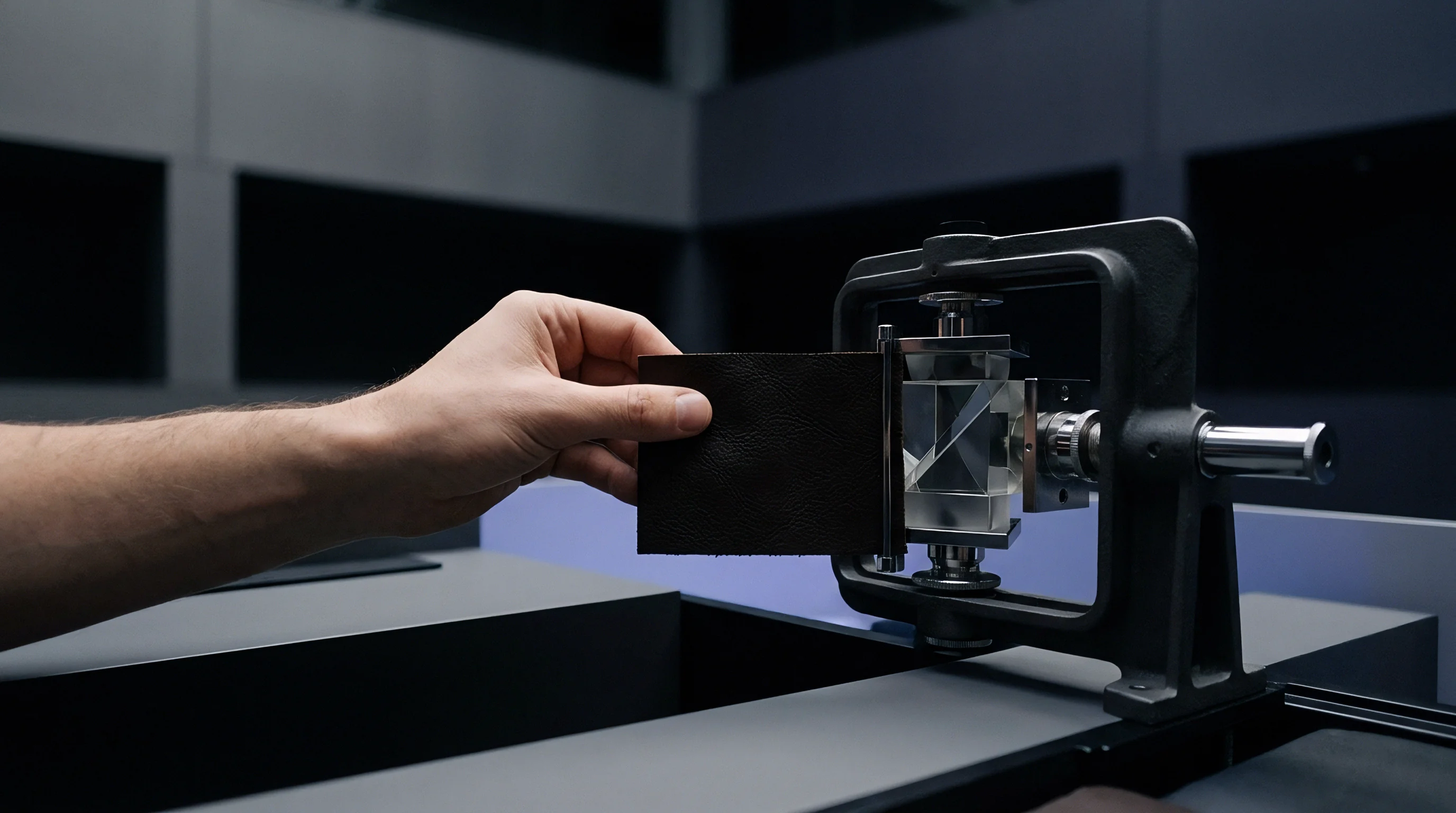

Audit
Incoming reel verification identifies packaging instability before expensive surface mount assembly begins. Quality audits on high-volume production lines demonstrate that supplier packaging quality varies across production batches, even from Tier 1 semiconductor manufacturers. Substrate thicknesses fluctuate by plus or minus 10 percent within standard manufacturing tolerances, while die attach epoxy fillet heights show substantial variation between automated dispensing nozzles.
An incoming component lot exhibiting marginal coplanarity will warp excessively during lead-free reflow, generating widespread analog front end register saturation across assembled circuit boards.
A package coplanarity specification tighter than thirty micrometers separates stable automotive-grade pressure sensors from commercial-grade components prone to severe solder-induced offset skew.
Procuring pressure sensors requires rigorous incoming inspection protocols to verify mechanical package integrity. Laser triangulation scanning and white-light interferometry profiling across sample reels reveal subtle package crowning or cupping prior to surface mounting. A sample lot showing more than 12 micrometers of room-temperature out-of-plane curvature across a 2.0 mm footprint indicates high internal residual stresses within the package substrate.
Feeding these stressed packages into a standard reflow profile results in severe warpage amplification, driving final board assembly failure rates above acceptable commercial thresholds.

Incoming Lot Sampling and Thermal Baseline
Optical profilometry measurements taken across bare sensor packages before reflow establish a baseline flatness metric that isolates defective manufacturing lots. JEDEC JESD22-A104 thermal cycling testing verifies that internal die attach and substrate bond lines survive repeated thermal expansions without mechanical delamination. Incoming quality assurance protocols require evaluating at least 32 sample components per reel batch under simulated reflow conditions, measuring room-temperature coplanarity before and after a standard IPC/JEDEC J-STD-020 lead-free temperature profile.
Lots exhibiting greater than 15 micrometers of post-reflow permanent plastic deformation must be quarantined immediately to prevent line contamination.
Evaluating package integrity under thermal exposure requires monitoring specific physical parameters that govern internal mechanical stability:
- Substrate glass transition temperature verification via differential scanning calorimetry confirms that the bismaleimide triazine core maintains structural rigidity up to 175 degrees Celsius.
- Die attach fillet height and coverage inspection using acoustic micro-imaging detects internal voids exceeding 15 percent of total die surface area.
- Package pin coplanarity measurement through automated optical inspection ensures all solder lands remain within a 25-micrometer planar envelope.
- Room temperature offset register baseline screening validates that unmounted parts report factory calibration values within plus or minus 30 Pascals of ambient barometric pressure.

Unit Cost Tradeoffs across Package Families
Package selection balances initial piece-part pricing against downstream assembly yields and firmware compensation overhead. A bare-die land grid array sensor represents the lowest upfront silicon expenditure, typically pricing between 0.85 and 1.35 US dollars in volumes of 50,000 units. This form factor imposes severe hidden integration costs, requiring expensive PCB slot routing, tight copper balance controls, and secondary post-reflow board calibration.
Conversely, pre-packaged gel-filled modules or ceramic standalone pressure transducers absorb mechanical stresses internally, bypassing board-level warpage entirely at the expense of a significantly higher piece-part unit cost.
Consider a typical commercial production run of 50,000 industrial IoT sensor assemblies. Sourcing a standard 2.0 mm by 2.0 mm bare LGA sensor at 0.95 US dollars yields a component bill of materials cost of 47,500 US dollars. Without routed board relief slots, reflow warpage generates an average 4.2 percent board failure rate during end-of-line functional pressure testing, scrap-costing approximately 28.50 US dollars per fully populated board assembly and resulting in 59,850 US dollars in scrapped product.
Implementing automated board-level pneumatic calibration on the assembly line recovers the failing boards, but amortizing the calibration chamber hardware and production cycle time adds 0.65 US dollars per unit in direct manufacturing expenditure. Sourcing a premium gel-filled LGA package at 1.45 US dollars increases upfront component procurement by 25,000 US dollars, yet it reduces assembly scrap rates to below 0.3 percent and eliminates the requirement for secondary factory recalibration cycles entirely.
| Package Configuration | Base Unit Price (USD) | Total Component BOM (USD) | Scrap Yield Loss (%) | Scrap Cost (USD) | Secondary Board Trim (USD) | Effective Landed Cost (USD) |
|---|---|---|---|---|---|---|
| Standard LGA (No PCB Slots) | 0.95 | 47,500 | 4.2 | 59,850 | 0 | 107,350 |
| Standard LGA (With PCB Relief) | 0.95 | 47,500 | 0.8 | 11,400 | 7,500 (NRE/Routing) | 66,400 |
| Standard LGA (Post-Reflow Trim) | 0.95 | 47,500 | 0.4 | 5,700 | 32,500 (Labor/Cycle) | 85,700 |
| Gel-Filled LGA Package | 1.45 | 72,500 | 0.3 | 4,275 | 0 | 76,775 |
| Ceramic Housed Standalone Module | 4.80 | 240,000 | 0.05 | 712 | 0 | 240,712 |
| Note: Assumptions reflect a fully loaded PCB assembly cost of 28.50 USD per unit, evaluated across 50,000 units on a standard automated SMT placement line. | ||||||
Invoking IPC-A-610 Class 3 coplanarity requirements within purchase agreements forces component distributors to guarantee package flatness within tighter physical tolerances before reels depart the factory floor.