Precision Analog Converter Substrate Gradient Strain Decoupling
Milled PCB isolation slots and compliant leaded packages attenuate board-level thermal gradient strain to preserve 24-bit converter offset accuracy.


Variant
A 24-bit delta-sigma converter die in a 4 mm by 4 mm quad flat no-lead housing lists at four dollars and twenty cents in ten-thousand-piece reels. That same physical silicon element mounted inside a thin shrink small outline housing with gull-wing leads commands five dollars and sixty cents from the same franchised distributor. When specified in a hermetic ceramic dual in-line package with gold-plated side-brazed pins, the quotation jumps to thirty-eight dollars per unit.
The thirty-three-dollar spread across these three commercial offerings purchases mechanical compliance. It buys the physical attenuation of substrate warping before circuit board bending moments reach the sensitive analog core.

Package Form Factors and Board Real Estate
Surface mount analog components distribute mechanical loads through their outer terminal geometry. Quad flat no-lead devices solder directly to copper lands through perimeter pads and an exposed thermal ground slug. The package sits flat against the laminate.
Solder joint heights rarely exceed fifty micrometers after convection reflow. Because the thermal expansion coefficient of standard FR-4 dielectric ranges from 14 to 18 parts per million per Kelvin while silicon expands at 2.8 parts per million per Kelvin, temperature shifts produce direct interfacial shear across the joint layer. Copper traces contract and expand against the silicon crystal with minimal mechanical relief.
Gull-wing leads introduce an external mechanical spring between the printed wiring board and the molded epoxy case. Thin copper-alloy lead frames formed into compliant outer feet flex under lateral and vertical displacement. Board bending forces that induce hundreds of microstrain in a bottom-terminated housing cause the gull-wing lead to bend elastically along its upper shoulder.
The silicon die inside the molded plastic experiences less than one-fifth of the external board flexure. Surface mount area expands from sixteen square millimeters for a twenty-four-pin QFN to forty-two square millimeters for a TSSOP equivalent. Designers trade component packing density directly against baseline electrical stability.
| Package Form | Terminal Construction | PCB Area (mm²) | Strain Transmission Factor | Unit Cost Index (QFN = 1.0) |
|---|---|---|---|---|
| QFN-24 (4×4 mm) | Bottom perimeter pads with exposed center pad | 16.0 | 0.82 | 1.00 |
| TSSOP-24 | Gull-wing formed copper alloy leads | 42.5 | 0.16 | 1.33 |
| SOIC-24 (Wide) | Extended gull-wing lead frame | 115.0 | 0.08 | 1.55 |
| LFBGA-36 (0.8 mm pitch) | SAC305 solder spheres (0.45 mm diameter) | 36.0 | 0.45 | 1.85 |
| Ceramic DIP-24 | Through-hole side-brazed Kovar pins | 185.0 | 0.02 | 9.05 |

Delivered Yield against Factory Calibration Expense
Production testing lines reveal shift errors when circuit cards undergo in-circuit functional checkouts. A converter calibrated at wafer probe exhibits zero-scale offset shifts when soldered down to a multi-layer board. Stiff packages transmit local laminate warping directly into internal bandgap references.
If a product specification calls for sub-microvolt DC stability across temperature, post-assembly factory calibration becomes mandatory for rigid package configurations. Running each assembled card through a two-temperature calibration chamber adds eighty seconds to cycle time. Across an annual run of fifty thousand units, that factory overhead exceeds forty thousand dollars in test equipment amortization and labor.
Gull-wing options absorb board stress silently. They retain factory wafer-trim accuracy through assembly.
- Quad flat no-lead packages eliminate compliant leads, transmitting sixty to eighty percent of board shear into the silicon crystal.
- Thin shrink small outline packages incorporate gull-wing terminals that deflect mechanically under thermal expansion.
- Ceramic dual in-line packages decouple board stresses through high standoff heights and rigid ceramic bases. Their unit price exceeds plastic equivalents by a factor of eight.
- Ball grid array packages distribute stress across perimeter solder spheres, generating localized shear at corner balls.
Skimping on mechanical isolation during layout forces subsequent revision respins and adds fifty thousand dollars in factory recalibration software hours.


Coupling
Thermal mismatch between printed circuit materials and semiconductor crystals creates localized shear distributions during operating cycles. The converter die bonds to a copper lead frame paddle with epoxy adhesive. Mold compound encapsulates the top surface.
Solder attaches the copper leads to FR-4 laminate. Each layer possesses a unique coefficient of thermal expansion, elastic modulus, and glass transition temperature. When heat dissipates from adjacent field-effect transistors, the laminate expands outward faster than the encapsulated silicon.
The solder joints pull the package corners outward, bowing the die into spherical curvature. Mechanical stress transfers into active transistor diffusions.

Silicon Piezoresistive Response in Voltage References
Internal bandgap circuits rely on paired bipolar junctions whose base-emitter differentials shift under mechanical compression. Silicon exhibits piezoresistive effects where mechanical strain alters the energy band valleys, changing charge carrier mobility and resistivity. Longitudinal and transverse piezoresistive coefficients in standard (100) silicon reach up to negative 102.2 times ten to the negative eleventh square meters per Newton along the crystal orientation.
Compression along this axis shifts matching between critical current mirror transistors. The converter reference output drifts by thirty to one hundred parts per million when package stresses reach fifty megapascals. Thin-film nichrome resistors maintain lower piezoresistive coefficients than diffused polysilicon structures, yet package shear twists matched resistor ladders out of geometric alignment.
Non-linearity errors manifest as mid-scale bowing across analog-to-digital transfer functions.
Asymmetric board warpage transforms isotropic thermal expansion into directional shear stress across the analog resistor ladder.
Stress creates offset voltage shift. Silicon cracks under tension.

Copper Imbalance and Asymmetric Flexure Vectors
Multilayer stackups with uneven plane distributions warp under heat dissipation from adjacent linear regulators. A printed circuit board containing four signal layers and two heavy ground planes experiences bending moments if copper area density differs across internal dielectric layers. Copper pours pull unevenly.
When an analog converter sits near a board edge or mounting screw, chassis fasteners lock the perimeter in place while the card interior expands. The converter package experiences combined bending and torsion.
- Piezoresistive coefficients govern resistance changes in diffused silicon resistors when compressive stress alters carrier mobility.
- Bandgap junction asymmetry introduces differential emitter-base voltage shifts exceeding twelve microvolts under fifty megapascals of uniaxial stress.
- Die attach adhesives provide uneven mechanical boundary conditions when voiding exceeds ten percent of total surface area.
- Silicon substrate thickness determines the flexural rigidity of the converter die under out-of-plane substrate bending moments.
Component vendors state in application notes that board-level strain falls outside datasheet parameter guarantees.


Slit
Milled isolation routings sever mechanical stress transfer paths through the dielectric substrate. Routing narrow slots through the circuit card around precision analog silicon blocks bending moments generated by mounting fasteners, connector insertion forces, and asymmetric thermal expansions. Strain waves traveling across the circuit board reflect off the open air boundary created by the routed perimeter.
The slot acts as an acoustic and mechanical open circuit within the laminate plate. By directing mechanical energy around the sensitive component island, surface microstrain at the converter solder joints drops from several hundred microstrain to single-digit background noise.

Why Do Perimeter Rout Slots Warp during Reflow?
Thermal expansion differences during solder assembly twist narrow unsupported circuit tongues. When a high-speed router bit removes laminate material to form a U-shaped slot around an analog converter, the remaining tongue of FR-4 remains attached by a single narrow neck. During the liquidus phase of reflow soldering, surface tension from molten solder on surface traces exerts torque on the tongue.
Unsupported cantilever tabs bow upward or downward by up to one hundred fifty micrometers if internal copper foil distribution lacks vertical symmetry. Copper balance prevents tab tilt. If the top layer contains eighty percent copper fill while the bottom contains twenty percent, the tongue warps during cooldown from 240 degrees Celsius.
Perimeter isolation routing attenuates board-level mechanical flexure strain by thirty-two decibels when slot width equals two millimeters.
Slot machining requires precise geometric dimensioning. Unbalanced copper generates asymmetric twist.
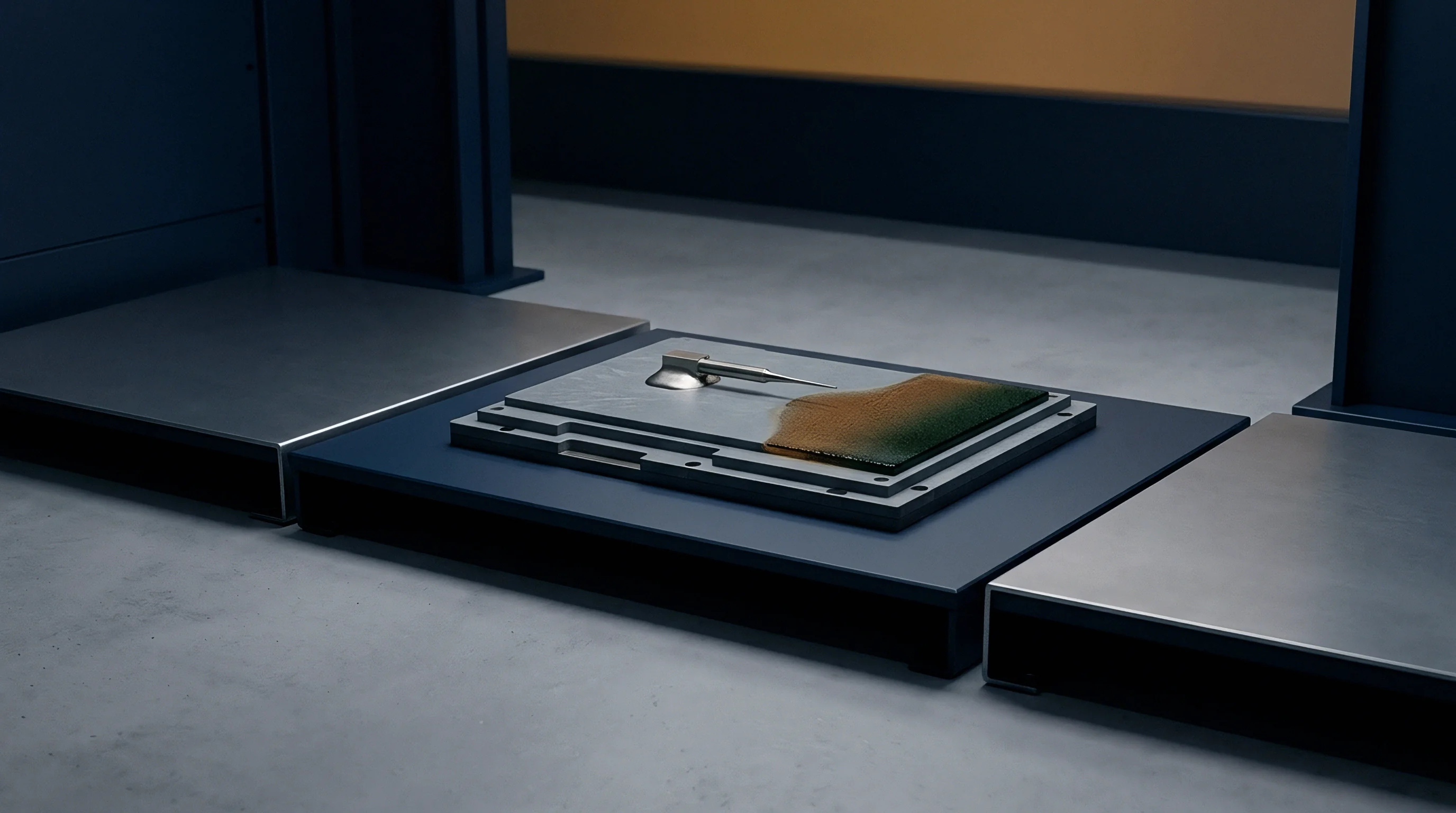
Mechanical Attenuation of Substrate Cantilever Tabs
Placing precision components on an isolated tongue suspended by a narrow neck shields sensitive internal circuits from chassis torque. Cantilever geometry determines mechanical compliance. Increasing tongue length raises compliance, isolating the converter from high-frequency board vibrations.
Increasing neck width raises mechanical stiffness, lowering deflection under gravitational acceleration. Designers balance shock survival against strain isolation. A slot width of one point six millimeters allows standard router bits to clear debris without loading cutters during panel breakout.
Milled slots sever thermal paths.
- Route perimeter relief slots with a minimum width of one millimeter to prevent solder bridging during wave or selective soldering.
- Position the converter die on a cantilever tongue supported by a single connecting neck aligned with the axis of minimum PCB curvature.
- Terminate router paths using circular relief drill holes measuring one point five millimeters to eliminate stress-concentrating sharp corners.
- Balance internal copper planes across the isolation bridge to prevent thermal warpage during the reflow cooling cycle.
| Slot Configuration | Slot Width (mm) | Connecting Neck Width (mm) | Strain Attenuation (dB) | First Natural Frequency (Hz) |
|---|---|---|---|---|
| Solid Board (No slot) | 0.0 | N/A | 0.0 | 1420 |
| Single Linear Slit | 1.2 | N/A | 12.4 | 1180 |
| C-Shaped Route (Three-sided) | 1.6 | 6.0 | 28.5 | 410 |
| Deep Cantilever (Three-sided) | 2.0 | 3.5 | 36.2 | 185 |
| Full Island (Two torsion bridges) | 1.6 | 3.0 (x2) | 31.0 | 520 |
| Data evaluated on 1.6 mm thick FR-4 four-layer laminate under 500 microstrain four-point bend deflection. | ||||
A slot cut between a heat source and a precision converter keeps the measurement baseline steady.


Standoff
The vertical gap between the package underbelly and the mounting land fixes the mechanical compliance of the electrical interconnection. Solder joints act as structural columns connecting package pads to laminate lands. Total shear strain in a solder joint equals the relative lateral thermal displacement divided by the joint standoff height.
Increasing standoff from thirty micrometers to eighty micrometers cuts shear strain in half for an identical thermal gradient. Component placement accuracy and solder paste stencil design govern this dimension across production lots. Solder creep relaxes initial pre-load.

Which Solder Alloy Preserves Package Compliance?
Tin-lead metallurgy exhibits higher plastic shear accommodation than near-eutectic tin-silver-copper formulations under cyclical strain. Standard SAC305 alloy possesses an elastic modulus of approximately fifty-one gigapascals at room temperature. Eutectic Sn63Pb37 exhibits an elastic modulus of thirty-two gigapascals.
Slower intermetallic compound growth in tin-lead joints prevents premature grain boundary embrittlement. Leaded solder creeps under continuous board bending, slowly dissipating stress rather than transferring shear directly into the converter silicon die. RoHS exemptions for medical and aerospace instrumentation permit leaded alloys specifically to preserve measurement integrity in extreme operating environments.
Solder alloys exhibit strain-rate sensitivity. Corner pads bear peak stress.
| Alloy Designation | Composition | Melting Point (°C) | Modulus (GPa) | Creep Compliance (1/GPa) |
|---|---|---|---|---|
| SAC305 | Sn96.5 Ag3.0 Cu0.5 | 217 – 220 | 51.0 | 0.012 |
| Sn63Pb37 | Sn63 Pb37 | 183 (Eutectic) | 32.5 | 0.038 |
| Bi58Sn42 | Bi58 Sn42 | 138 (Eutectic) | 44.0 | 0.006 |
| In97Ag3 | In97 Ag3 | 143 (Eutectic) | 10.5 | 0.145 |
Compliance with IPC-9701 thermal cycling criteria forces qualification testing across one thousand cycles from minus forty to one hundred twenty-five degrees Celsius.
Underfill Elasticity and Thermal Shear Transfer
Capillary encapsulants lock the component base to the circuit card, transmitting laminate expansion into the sensing core. Epoxy underfills were originally engineered to support flip-chip BGA joints against thermal fatigue drop shock. In high-resolution analog conversion circuits, rigid underfills degrade offset performance.
When an epoxy underfill with an elastic modulus of eight gigapascals cures beneath a QFN package, it couples the thermal expansion of the board directly across the full surface area of the exposed pad. High stiffness accelerates trace fracture. Reworking an underfilled converter requires heating the board to two hundred degrees Celsius and scraping cured resin, which destroys copper pads.
Low-modulus silicone encapsulants with elasticity values under five megapascals cushion the die against moisture while decoupling thermal shear.
Contract manufacturing agreements citing IPC-A-610 Class 3 heel fillet criteria prevent unauthorized reductions in paste stencil thickness.


Screening
Production testing procedures evaluate converter offset drift by applying controlled deflection to populated circuit assemblies. Test fixtures verify that mechanical isolation slots and lead geometries hold electrical calibration limits under real-world handling loads. Pneumatic bed-of-nails clamps push against peripheral board edges while digitizers record converter output codes.
If an analog-to-digital converter shifts more than two least significant bits when the card experiences three hundred microstrain of bending, the assembly fails screening. Board warpage limits determine qualification pass rates. Asymmetry drives long-term zero drift.
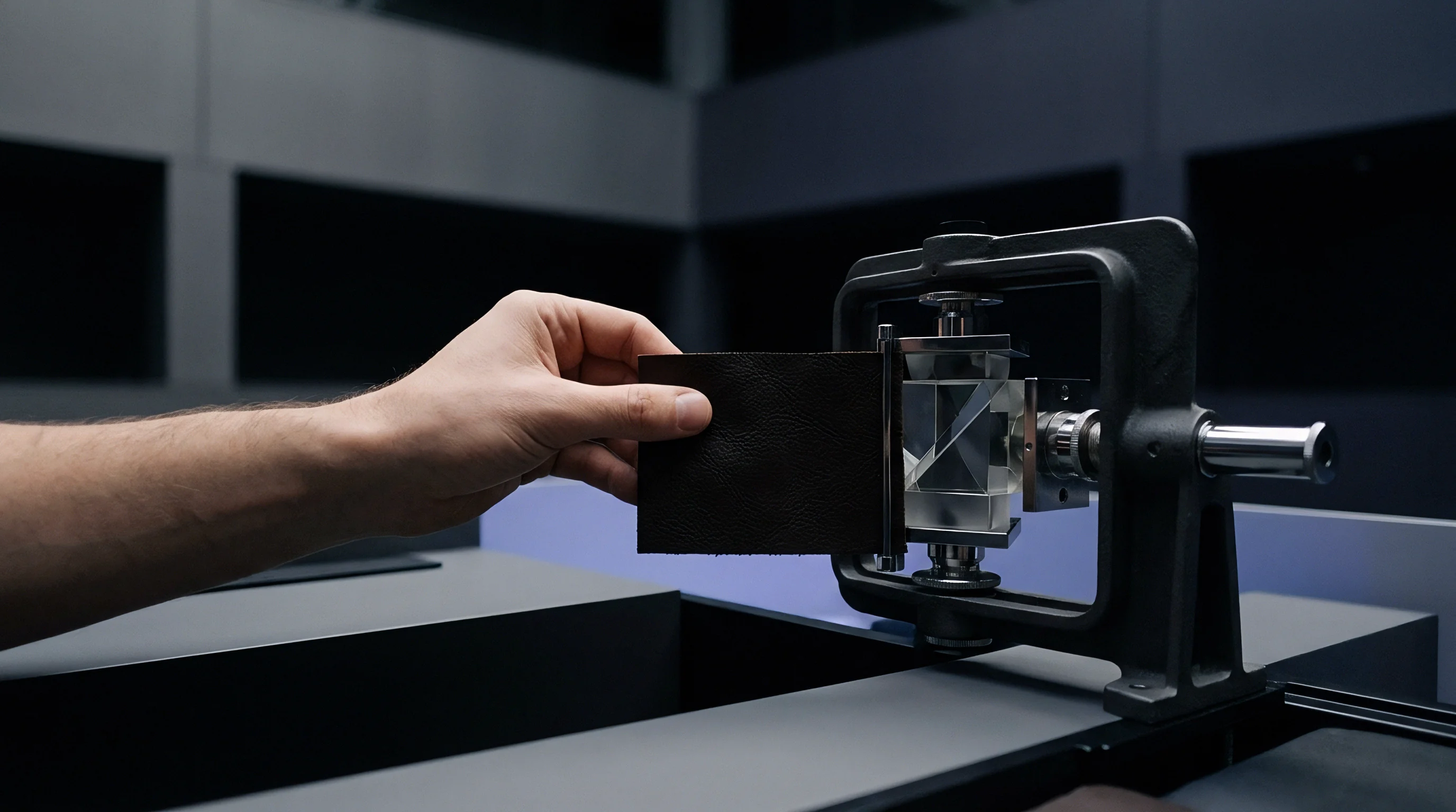
Strain Gauge Profiling on Populated Panels
Triaxial rosette sensors placed adjacent to component corners record microstrain levels during depaneling and functional testing. Standard IPC-JEDEC-9704 defines destructive test limits for surface-mounted electronic components on printed boards. For thin quad packages, diagonal strain rates during depaneling router operations must remain below five hundred microstrain per second to protect against internal die delamination.
Precision 24-bit converters demand tighter working limits. Zero-scale drift begins at fifty microstrain. Rosette gauges confirm that router breakout tabs sit far enough from sensitive analog islands to prevent transient shock during panel separation.
Calibrated offsets degrade over time.
Placing mounting screws near precision converters guarantees calibration shifts under chassis vibration.

Long-Term Offset Settling and Drift Sign-Off
Post-assembly aging shifts converter outputs across initial thermal exposure cycles as structural stresses relax. Solder joints undergo room-temperature grain coarsening during the first forty-eight hours following convection reflow. Solder creep relieves internal residual stresses locked into the copper leads during cooling.
During this metallurgical settling phase, analog converter zero-scale offsets migrate by up to ten microvolts. Automated burn-in cycles running boards through five thermal cycles between zero and seventy degrees Celsius stabilize the solder microstructure before baseline calibration recording. Gold wires detach during flexure.
Field data from downhole drilling tools, weigh scale instrumentation, and industrial process control transmitters confirm that analog front-ends isolated by routed perimeter slots maintain initial zero-scale calibration across five years of field deployment. Solid laminate layouts suffer continuous baseline drift as enclosure fasteners relax, humidity swells FR-4 resin, and adjacent power components degrade board flatness over thousands of operating hours.
Engineers still dispute whether software compensation algorithms can reliably track nonlinear mechanical hysteresis across a ten-year operating life.