
Precision Bandgap Thermal Stress Error Reduction across Surface Mount Packages
Mitigate bandgap thermal stress errors using compliant leaded packages, PCB isolation slots, polyimide die buffers, and stabilized factory calibration.
Mitigate bandgap thermal stress errors using compliant leaded packages, PCB isolation slots, polyimide die buffers, and stabilized factory calibration.

Mitigate surface-mount precision reference thermomechanical drift using three-sided PCB slot moats, compliant land patterns, or hermetic ceramic packages.
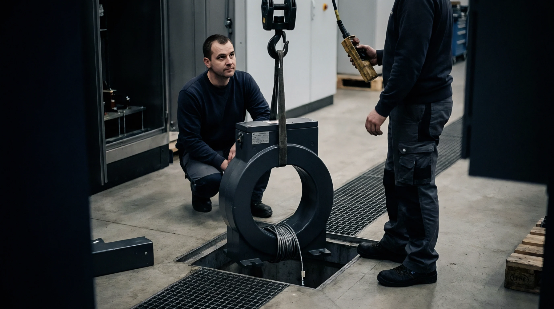
Precision voltage reference accuracy depends on isolating packages from board flexure, balancing trace Seebeck junctions, and blocking thermal conduction paths.

Board flexure stress couples to analog dies via solder joints and mold compounds, shifting bandgap voltages up to 10 millivolts under thermal cycling.

Asymmetric thermal gradients across precision references induce microvolt offsets through Seebeck potentials and piezo-resistive stress imbalance.

Monolithic reference thermal drift sensitivity combines silicon junction non-linearities, piezoresistive mechanical package stress, and solder reflow hysteresis.

Active buffers isolate bus capacitance beyond 400 picofarads by segmenting traces and using static voltage offsets or edge accelerators to meet timing limits.
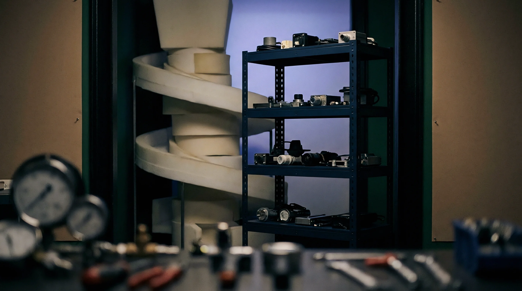
Internal bandgap voltage errors in high gradient layouts are reduced by common-centroid matching, thermal isolation trenching, and package stress mitigation.
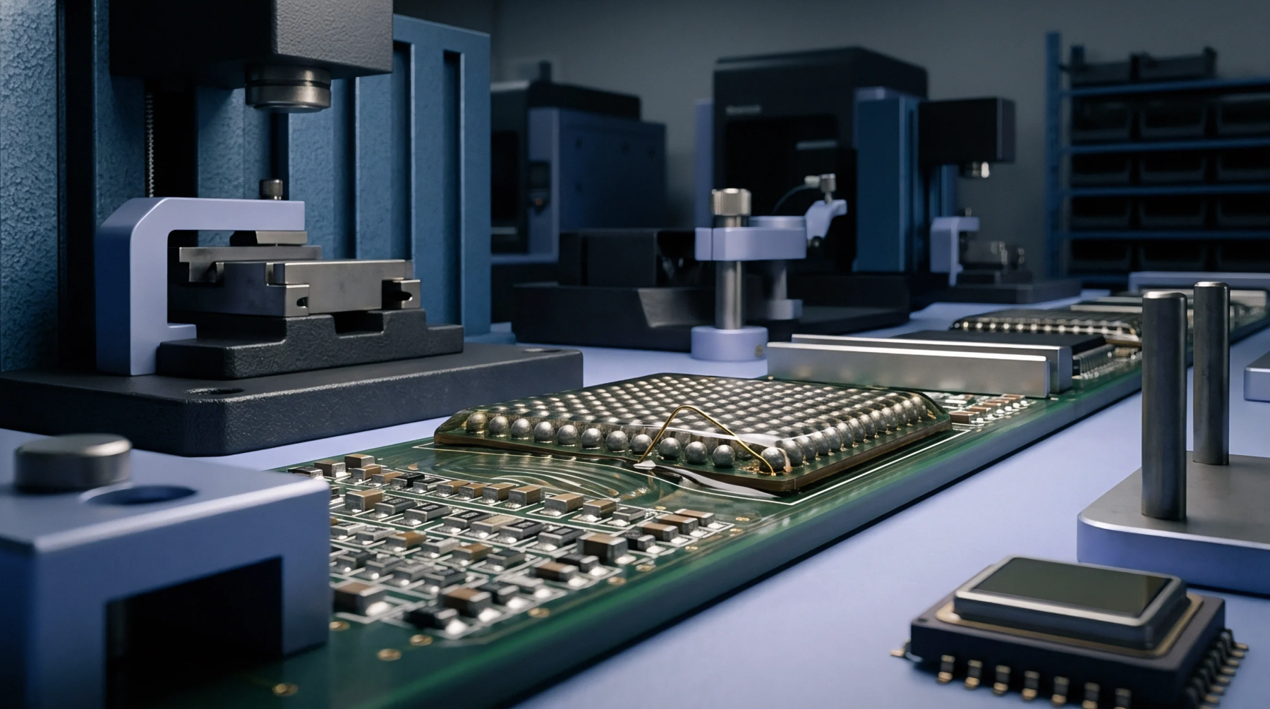
Isothermal precision reference layouts eliminate microvolt thermal EMFs and mechanical strain by balancing copper symmetry, milling strain-relief cuts, and decoupling heat flow.

Asymmetric output load dissipation creates substrate thermal gradients across monolithic reference dies, inducing microvolt baseline offsets in precision data converters.
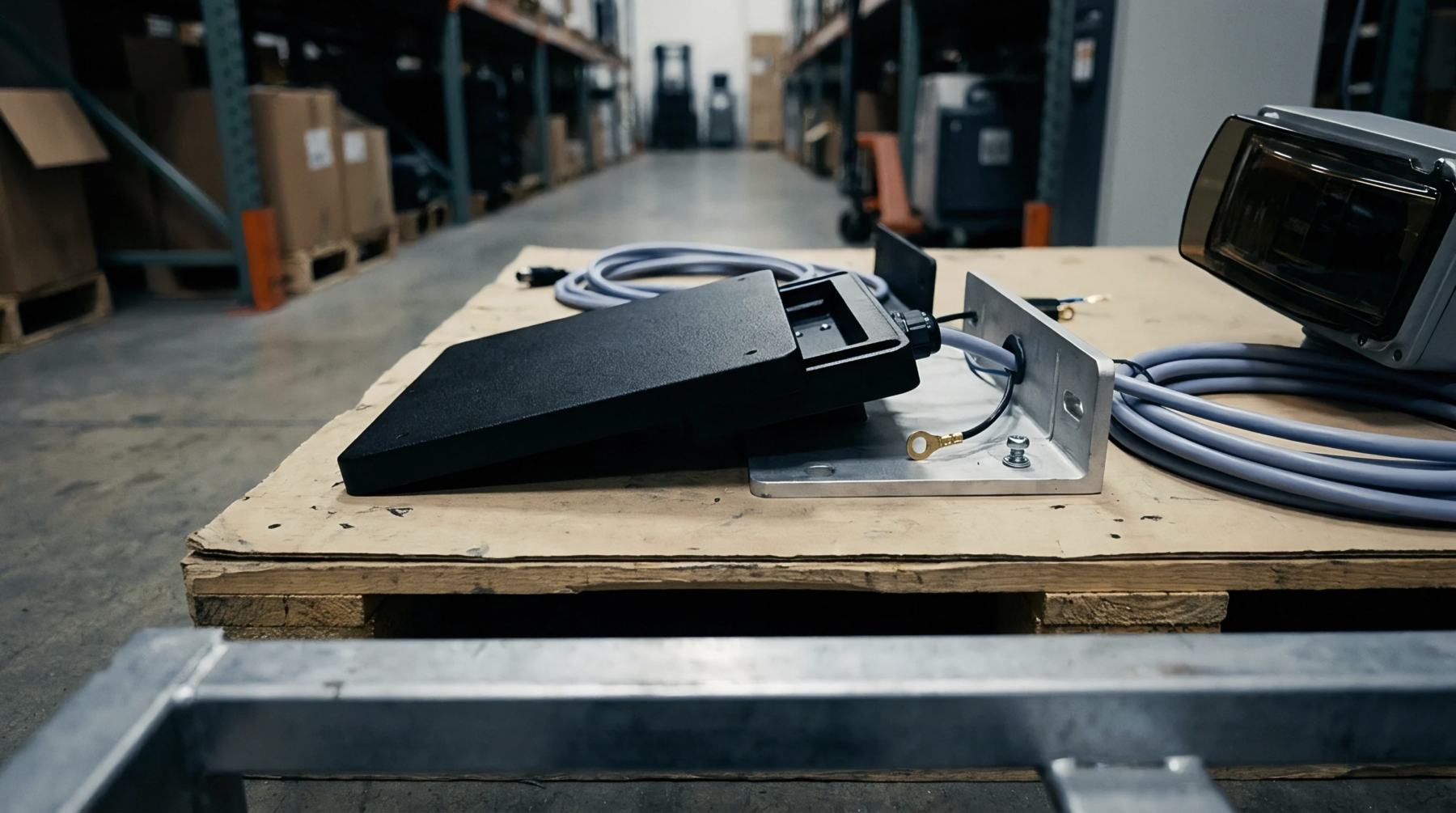
Enforce 18-month EOL notice timelines and silicon-level allocation guarantees to protect sensor supply chains from unannounced component discontinuances.

External loading on internal voltage references degrades system precision through load droop, substrate thermal gradients, and capacitive loop instability.
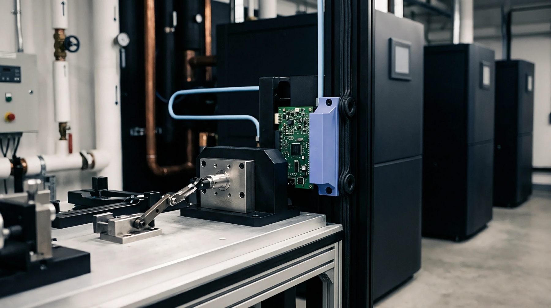
Board flexure transfers shear strain through solder joints into silicon dies, shifting zero-point offsets; isolate footprints using slots or diagonal placement.
Expertise is a utility, not a secret. sentiention™ publishes its working knowledge as open reference: intelligence layer covering the materials it sources, the markets it enters, and the reference that serves both.