Package Format
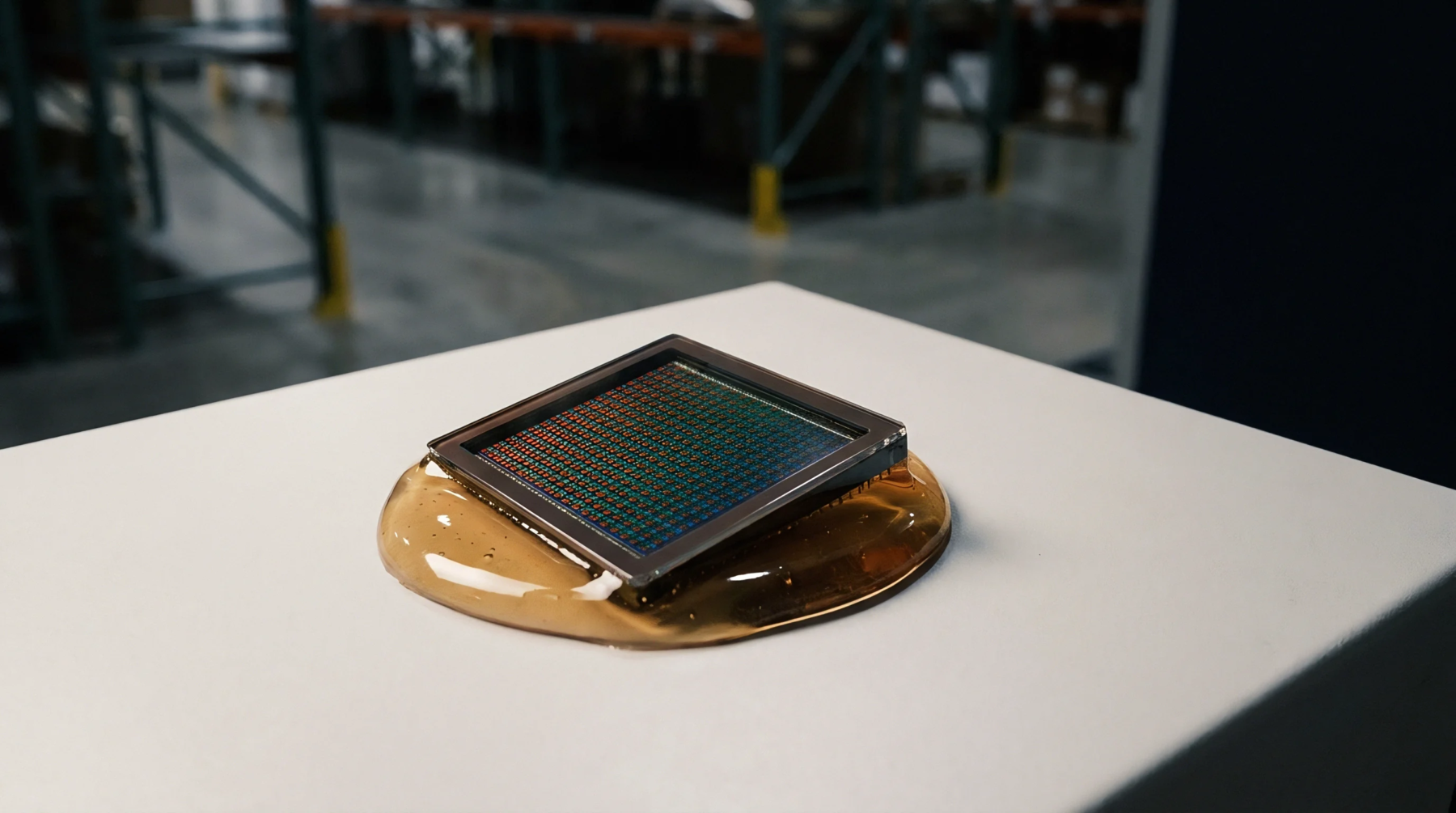
Surface mounted ceramic housings protect integrated circuits without the use of metal pins or protruding legs. The leadless chip carrier utilizes conductive pads on its underside to establish electrical contact with the printed circuit board.
Surface Interconnect
Connection points reside along the edges or across the bottom surface of the ceramic body. Solder fillets form between these pads and the board traces during the reflow process.
Thermal Management
Heat dissipation occurs through the bottom of the package directly into the circuit board. A leadless chip carrier often includes a large central pad to improve the transfer of thermal energy away from the silicon die.
Mechanical Solder
Reliability of the electrical connection depends on the quality of the solder joints. Because there are no flexible leads to absorb mechanical energy, the leadless chip carrier is susceptible to fatigue if the board undergoes significant bending. Designers often use specialized underfill materials or high transition temperature circuit boards to mitigate this risk.
Solder thickness must be carefully controlled to provide enough compliance for thermal expansion. Inspection of the joints typically requires automated optical or x-ray systems to ensure that the solder has wetted the pads correctly. The low profile of this housing makes it suitable for high density electronics where vertical space is restricted.