
Stress Decoupling Buffer Selection for Piezoresistive Pressure Sensor Packaging
Stress decoupling buffers isolate piezoresistive pressure sensor dies from thermal expansion and board flexure, preserving baseline zero-offset calibration stability.
Stress decoupling buffers isolate piezoresistive pressure sensor dies from thermal expansion and board flexure, preserving baseline zero-offset calibration stability.
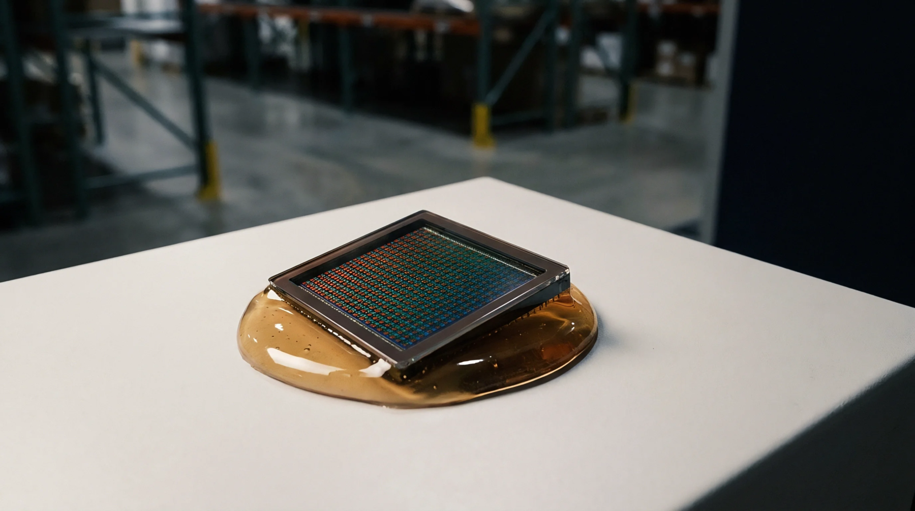
Polymer encapsulation selection requires matching matrix CTE and modulus to die silicon to prevent parametric drift while maintaining moisture barrier limits.
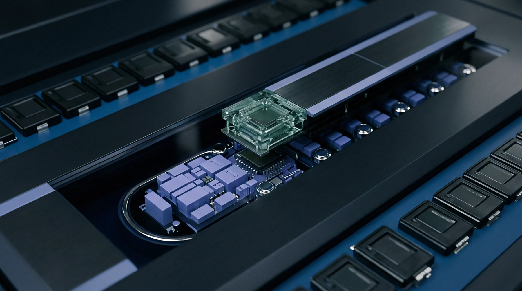
Dynamic calibration fixtures must balance micro-cavity fluid acoustic matching with thermal gradient insulation to achieve stable, high-throughput testing.

Mitigate interfacial shear stress in cavity sensor packages by matching substrate thermal expansion and applying low-modulus decoupling layers.
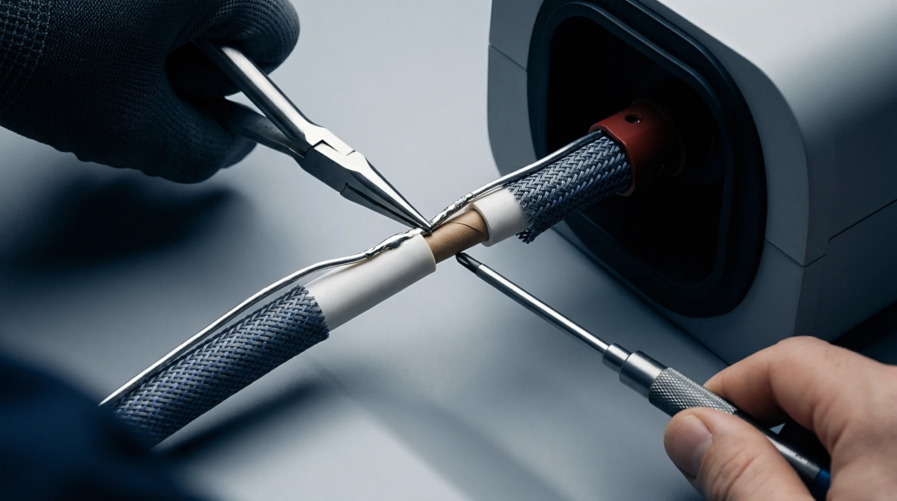
Decouple piezoresistive diaphragm SMT mounting strain using borosilicate pedestals, symmetrical land patterns, PCB relief slots, and delayed digital offset calibration.

High-temperature package signal integrity requires active compensation scaling and low-loss high-Tg dielectrics to offset severe thermal loss expansion.
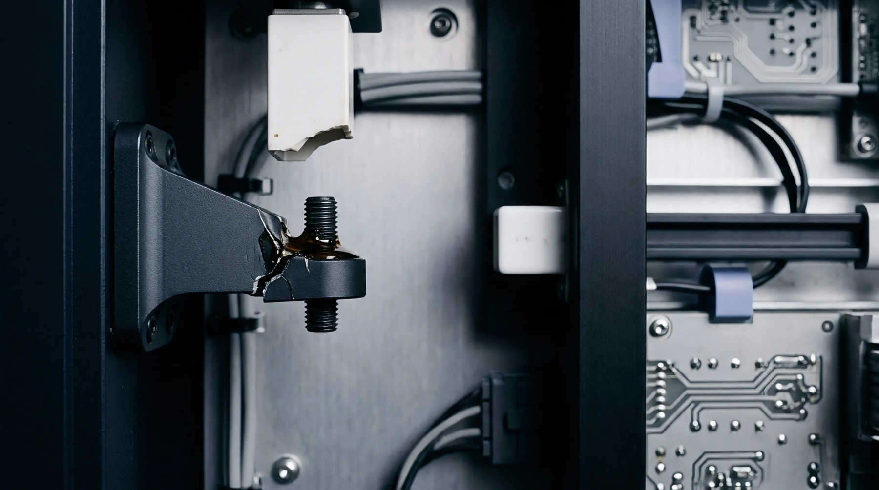
Managing Fast Mode Plus stray capacitance requires low capacitance trace layout active pull up current sources and bus buffers to meet 120 ns rise times

Pull-up resistor sizing balances sink current limits against bus parasitic capacitance to guarantee rise times match speed mode specifications.
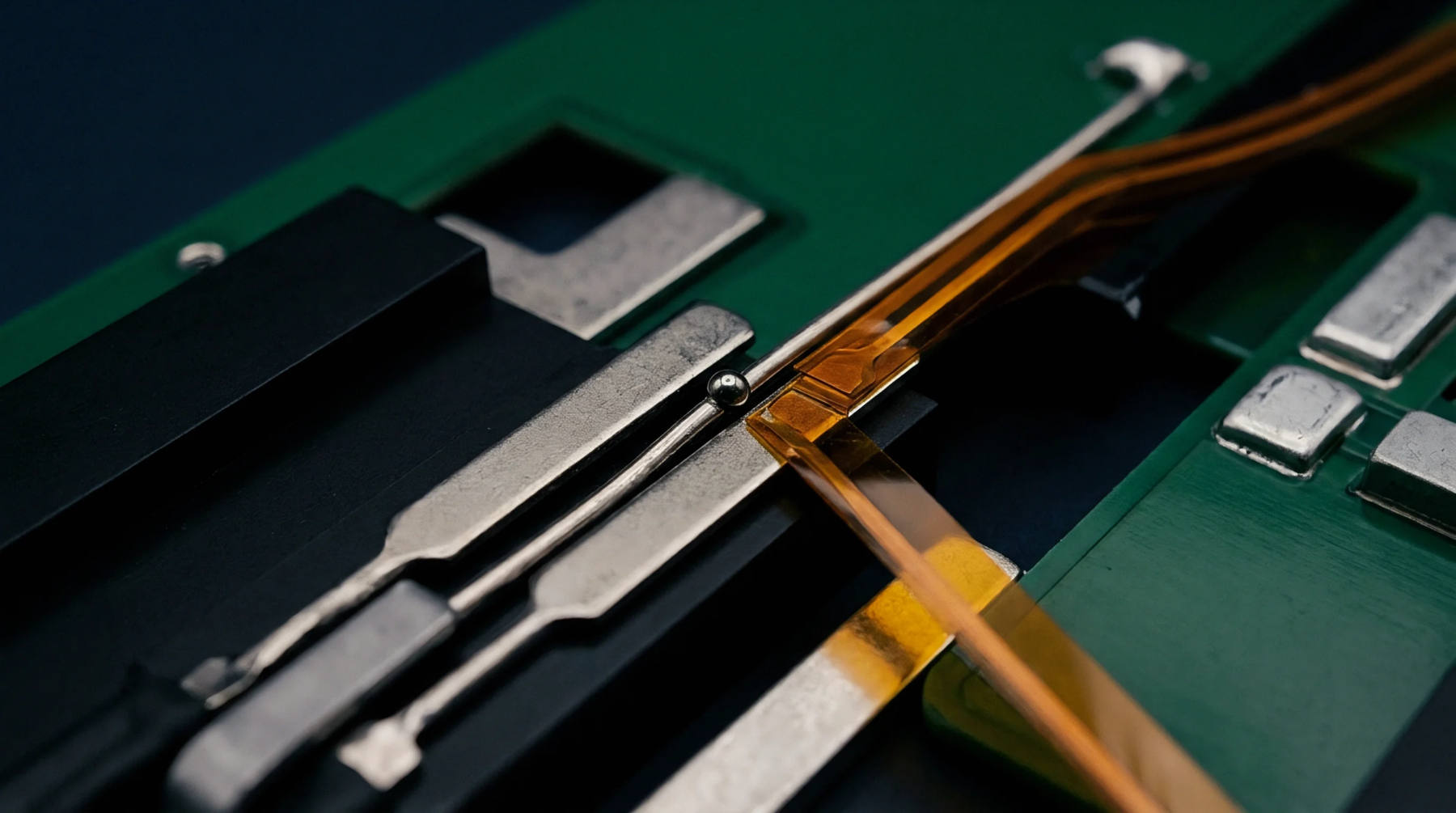
Board reflow micro strain shifts sensor zero offsets by consuming digital calibration headroom, requiring footprint symmetry and post-assembly dwell before trim.
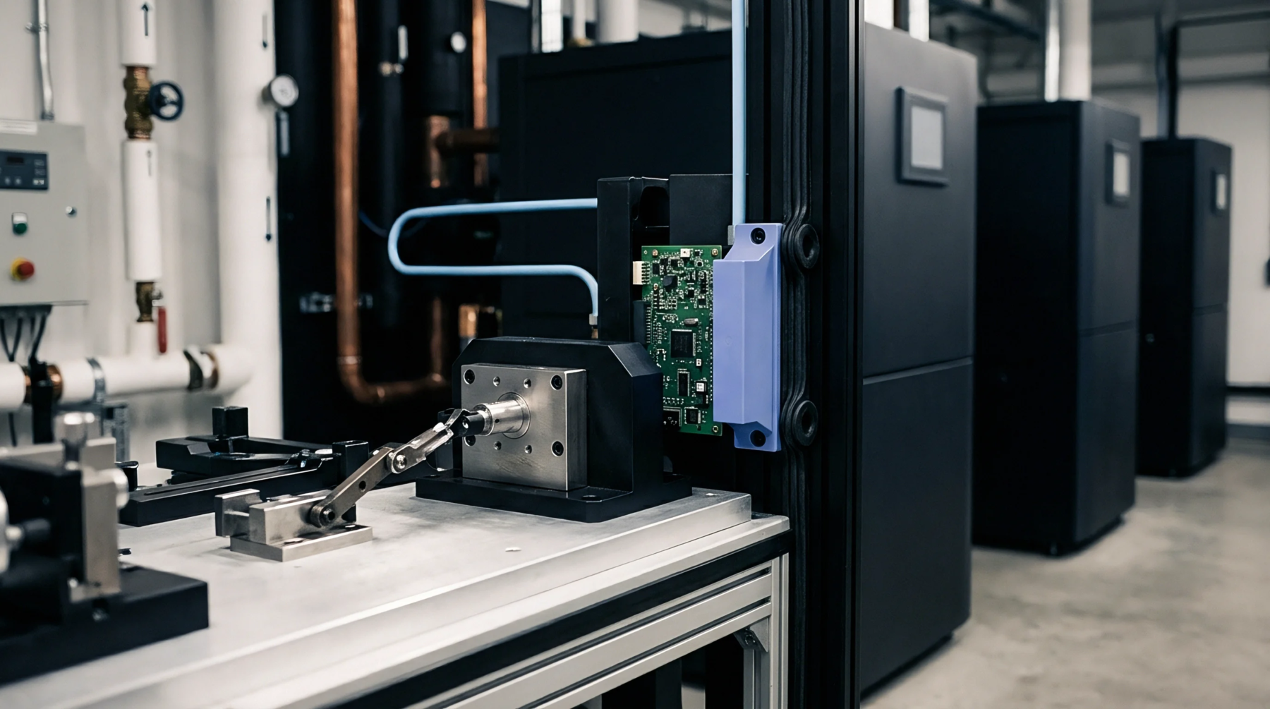
Solder mask aperture optimization balances registration tolerance against dam width to eliminate bridging and maintain solder joint mechanical integrity.

Land pattern calibration requires balancing IPC-7351 solder fillet dimensions against fabricator tolerance limits to maximize assembly yield and high-speed signal integrity.

Modeling solder viscoplastic creep relaxation predicts MEMS die strain and prevents long-term zero-point offset drift in surface-mounted sensor packages.

Exposed paddle QFN packaging introduces parasitic leadframe inductance and piezoresistive die strain drift, requiring unified electromagnetic-mechanical co-modeling.

Thermal pad solder voids reduce ground plane capacitance and raise thermal resistance, demanding matrix stencils and controlled reflow soak to preserve yield.

Buried microvia thermal fatigue causes gigahertz insertion loss drift before DC continuity breaks, requiring TDR testing to prevent high-speed link failures.

Solder voids over twelve percent under differential signal ground returns introduce local impedance drops that erode multigigabit channel margins.
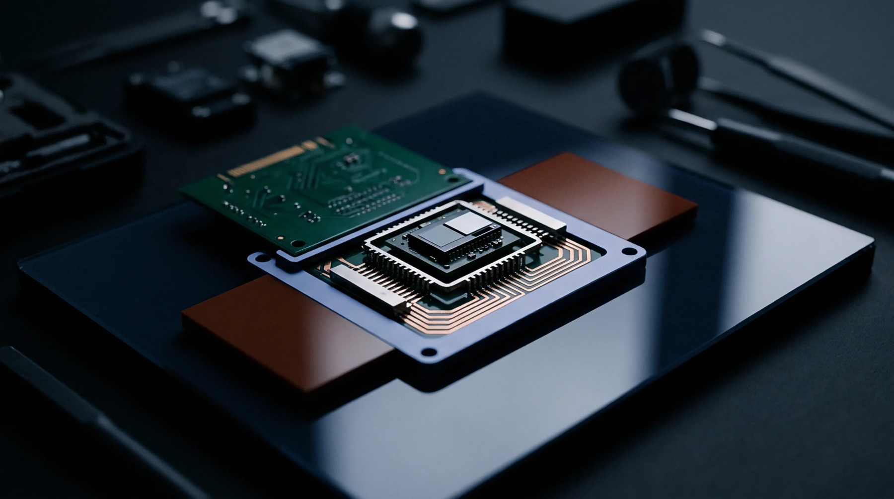
Specifying mold compound dielectric tolerances within plus or minus three percent prevents high-frequency interconnect impedance mismatches across production lots.

Differential trace discontinuities in high-speed sensor packages generate common-mode noise and timing jitter that require trace compensation and ground shielding.

Extracting QFN footprint inductance requires PEEC modeling of leadframe geometries and thermal via arrays to eliminate ground bounce in high-speed designs.
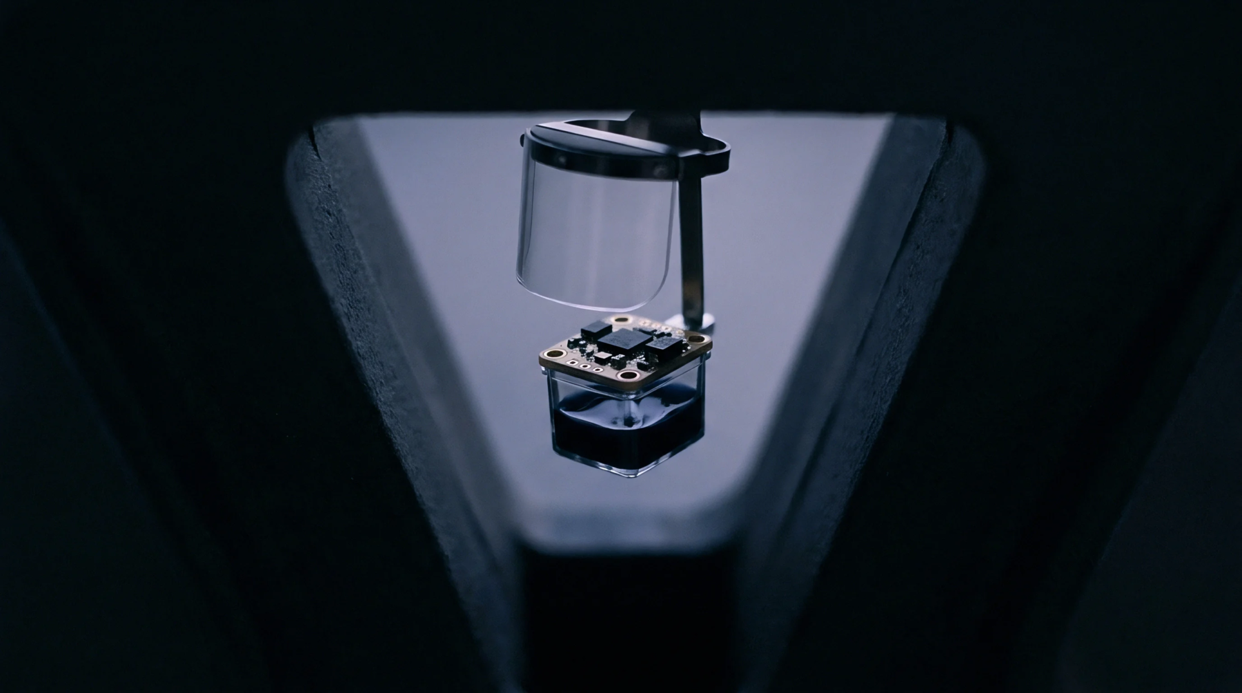
Leadless package integration requires balancing reduced lead inductance against increased PCB fabrication complexity, void management, and inspection costs.

Microalloying bismuth solders with antimony and nickel suppresses aged interfacial cleavage under impact by restricting intermetallic growth and bismuth segregation.

Strain rate matrices in explicit drop simulation prevent premature solder ball fatigue failure prediction by scaling material yield stress with impact velocity.
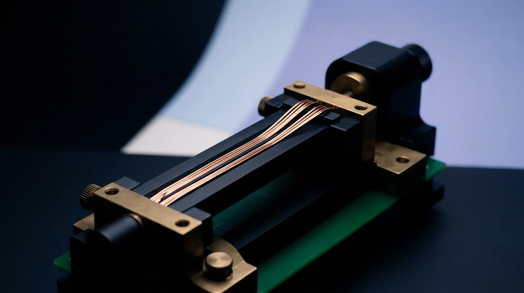
Bismuth segregation at copper intermetallic boundaries induces brittle cleavage under rapid drop shock, demanding microalloyed dopants to preserve high-velocity toughness.

Real-time microstrain vector integration requires synchronous 3-channel AFE sampling, deterministic CORDIC math execution, and dynamic IPC-9704 strain rate limit monitoring.
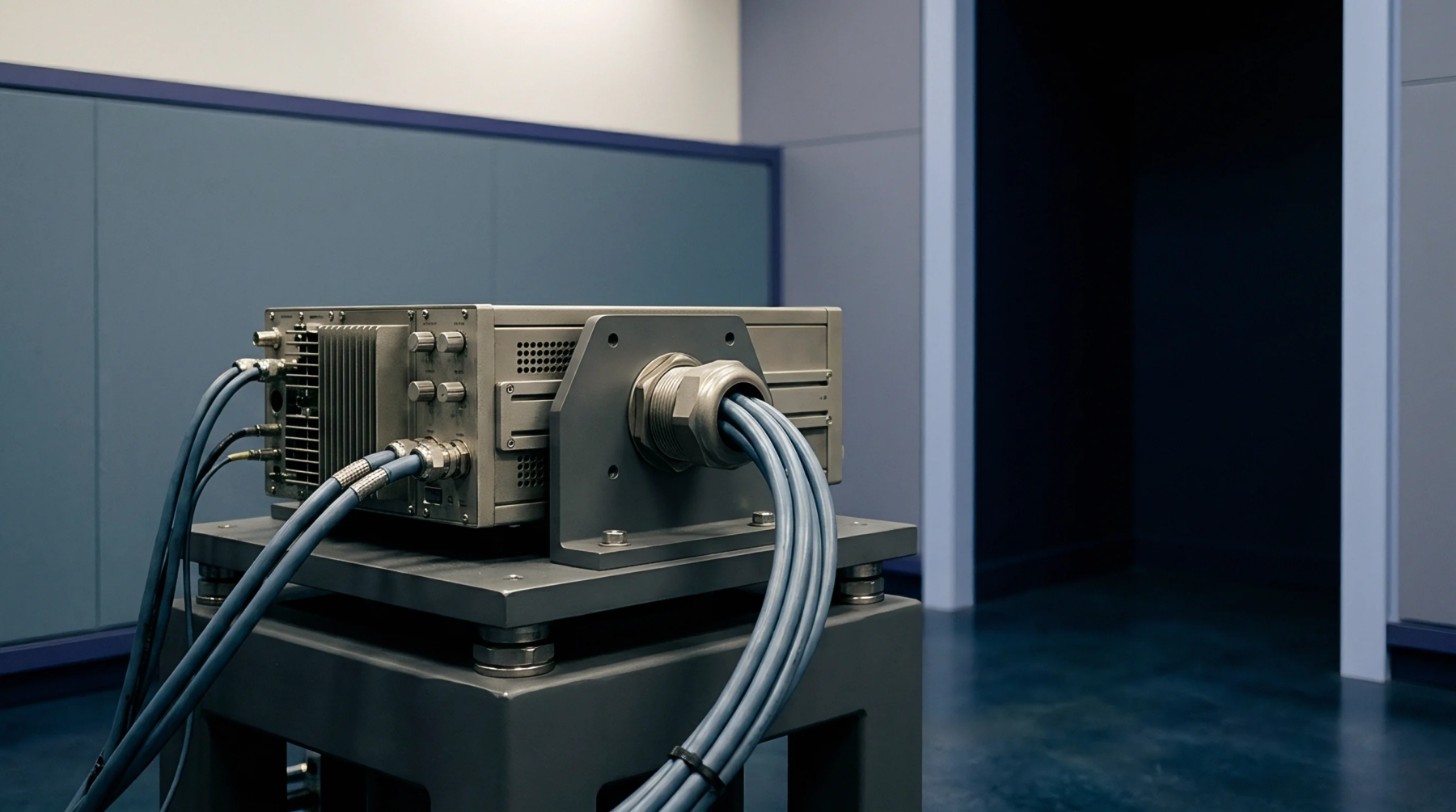
Auditable simultaneous ADC conditioning pairs active low-pass filtering with matched C0G passives to eliminate channel-to-channel phase skew under thermal load.

Matching rosette foil thermal expansion and enforcing bondline thickness below ten micrometers eliminates shear lag errors in surface strain measurements.
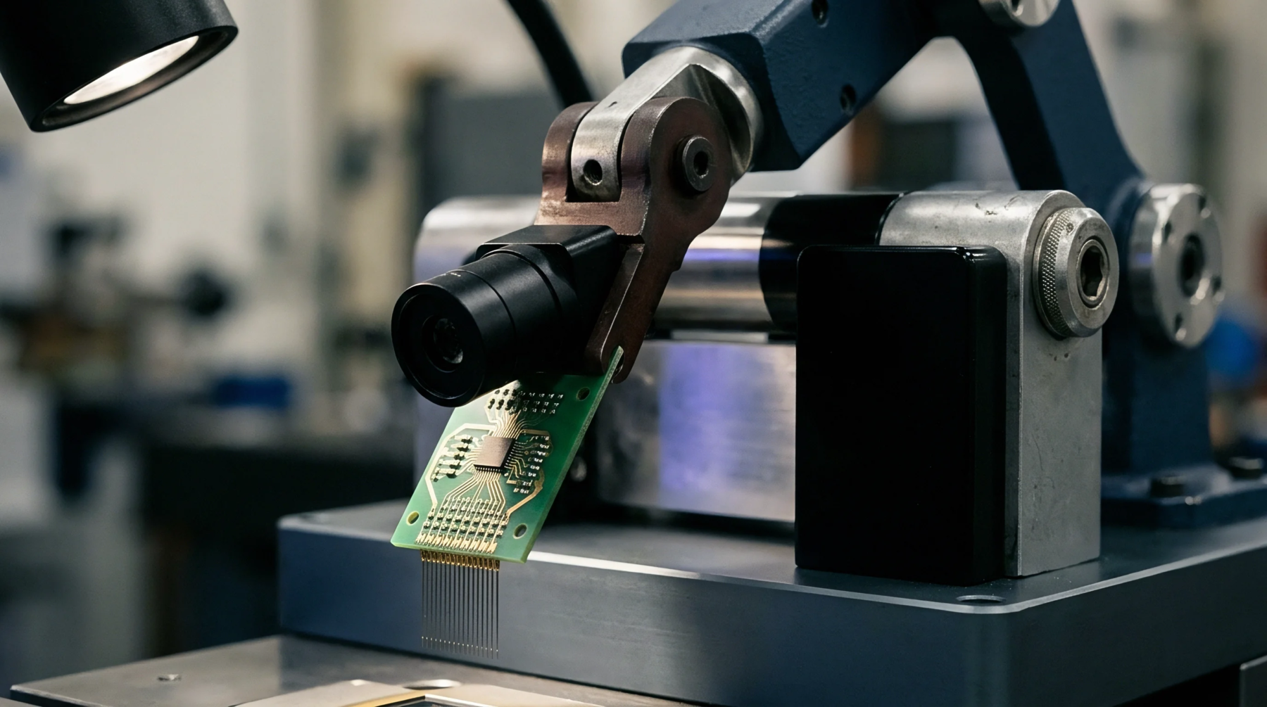
IPC/JEDEC strain compliance verification measures thermal reflow board strain with triaxial rosettes to prevent solder joint cracking and sensor offset drift.

Integrating piezoresistive strain gauges on HDI PCBs demands isolating thermal expansion mismatch while calibrating digital AFE registers post-reflow.
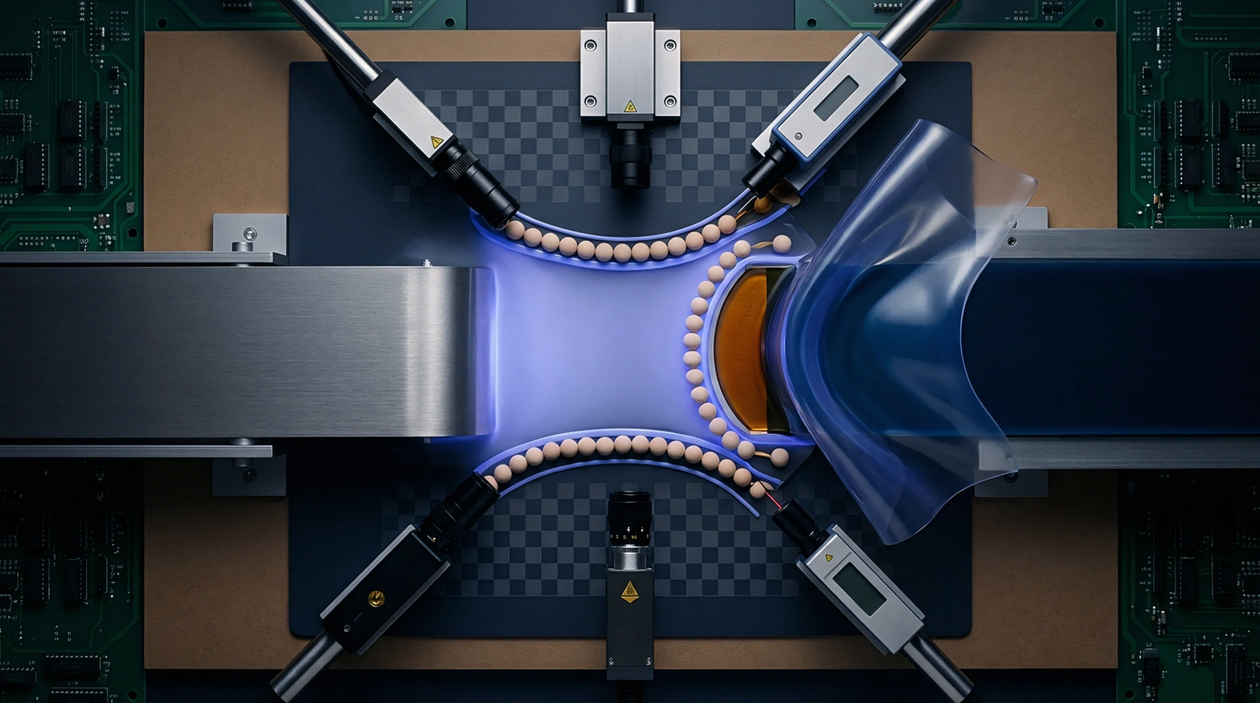
Verify ICT and depaneling strain rates below IPC/JEDEC-9704 dynamic limits using three-wire triaxial rosettes placed within two millimeters of package corners.

Multiaxial viscoplastic solder creep models predict package fatigue life by integrating rate dependent strain components under dynamic thermal gradients.
Expertise is a utility, not a secret. sentiention™ publishes its working knowledge as open reference: intelligence layer covering the materials it sources, the markets it enters, and the reference that serves both.