Thermomechanical Compensation Algorithms in High Speed Digital Pressure Sensors
Dynamic thermomechanical algorithms split pressure errors into steady polynomial drift and transient gradient terms, preserving millibar accuracy across fast thermal shocks.


Drift

Thermal Shock Induces False Pressure Transients
Rapid temperature changes distort high-speed digital pressure readings through mechanical stress rather than fluid pressure. A piezoresistive or capacitive micro-electro-mechanical diaphragm measures deflection, interpreting mechanical strain across the micromachined membrane as a barometric or hydraulic head. When a thermal transition sweeps across the component body at rates exceeding 5 degrees Celsius per second, thermal expansion mismatches between the silicon die, the glass or silicon pedestal, the die-attach adhesive, and the ceramic or molded substrate introduce differential physical shear.
This structural deflection reaches the active piezoresistors, altering electrical resistance through the piezoresistive effect. The integrated analog front end processes this piezoresistive deflection as a genuine change in process pressure. Static temperature lookup tables fail because the internal temperature diode and the mechanical diaphragm have distinct thermal masses, creating a dynamic thermal lag that generates transient measurement spikes during fast thermal steps.
High sample rate systems operating at 500 Hertz to 2 kilohertz reveal this mechanical divergence immediately. The onboard analog-to-digital converter digitizes raw diaphragm bridge voltage alongside an embedded substrate temperature diode. Static third-order polynomial compensation architectures assume steady-state equilibrium, applying coefficients derived from slow chamber calibrations.
During sudden temperature slew, the substrate temperature sensor responds with a thermal time constant ranging between 120 milliseconds and 450 milliseconds, whereas the micro-machined diaphragm, possessing a thickness under 10 micrometers, tracks ambient media temperature shifts in under 5 milliseconds. The physical mismatch between these two thermal response times generates an asymmetric compensation error. The digital engine calculates a temperature correction based on a delayed substrate reading, applying an incorrect offset adjustment to a diaphragm that has already experienced thermal expansion.
Transient spatial gradients across the die pedestal decouple the piezoresistor bridge temperature from internal reference diodes.
Board integration parameters compound this thermomechanical divergence. Surface-mount land patterns, solder volume variations, and structural copper layer distribution inside the host printed circuit board direct heat unevenly into the package terminals. The resulting directional heat flux induces a lateral gradient across the silicon surface.
A localized temperature difference of 0.8 degrees Celsius across a 1.2-millimeter piezoresistive bridge produces an uncompensated zero-point offset error reaching 2.5 hectopascals in low-pressure barometric components. Algorithms running inside the host microcontroller must separate the slow bulk temperature drift from high-frequency thermal transient vectors before applying mathematical correction matrices.
Uncompensated thermal transients corrupt closed-loop pneumatic controllers, triggering erroneous valve actuations that disrupt industrial process stability.


Hysteresis

Viscoelastic Die Attach Distorts Polynomial Fits
Die-attach materials introduce time-dependent stress relaxation that skews conventional polynomial compensation routines. Sensor fabricators mount the silicon pressure-sensing die to a glass pedestal or directly to a leadframe substrate using conductive epoxy or silicone adhesives. Silicone die-attach formulations feature low Young’s modulus, typically between 1.5 and 5.0 megapascals, which mechanically isolates the silicon element from printed circuit board warpage.
However, silicone exhibits significant viscoelasticity over wide operational bands from minus 40 degrees Celsius to 125 degrees Celsius. When exposed to rapid thermal transitions, the adhesive does not transfer thermal expansion stress instantaneously. The adhesive undergoes delayed physical relaxation, exhibiting a characteristic mechanical relaxation spectrum spanning tens of seconds.
Rigid conductive epoxies present an opposing operational compromise. Formulations possessing high glass transition temperatures and elastic moduli exceeding 3.5 gigapascals transfer package strain directly into the silicon bulk. As solder joints undergo plastic deformation during thermal cycling between extreme bounds, the cyclic shear forces transmit through the package leadframe, the cured epoxy bond-line, and into the active diaphragm perimeter.
This packaging mechanism creates thermal hysteresis loops in the digital pressure output. When cyclically tested across a thermal envelope of minus 20 degrees Celsius to 85 degrees Celsius, the uncompensated pressure baseline fails to trace identical trajectories during heating and cooling phases, leaving a residual divergence of 0.5 to 1.8 hectopascals at identical ambient temperatures.
Static factory calibration routines mask this phenomenon by measuring baseline values only after the unit stabilizes inside an environmental oven for fifteen minutes per setpoint. This steady-state factory procedure calculates trim coefficients stored in on-chip non-volatile memory registers. During field deployments, thermal stabilization rarely occurs, subjecting the sensor package to continuous environmental transitions.
The steady-state compensation model proves inadequate under dynamic thermal excitation because the instantaneous mechanical strain on the piezoresistors depends directly on the thermal history and the rate of temperature change.
| Adhesive Category | Elastic Modulus (MPa) | Glass Transition (°C) | Coefficient Thermal Expansion (ppm/K) | Thermomechanical Relaxation Time (s) |
|---|---|---|---|---|
| Standard Filled Epoxy | 6500 to 8500 | 110 to 145 | 35 to 55 | 0.05 to 0.20 |
| Modified Flexible Epoxy | 800 to 1800 | 45 to 70 | 65 to 110 | 1.50 to 4.20 |
| Soft Fluorosilicone | 1.2 to 3.8 | -65 to -40 | 220 to 340 | 12.0 to 45.0 |
| Low-Stress Dimethyl Silicone | 2.0 to 6.5 | -115 to -85 | 280 to 400 | 18.0 to 60.0 |
| Eutectic Gold-Tin (Au80Sn20) | 59000 to 68000 | 280 | 16 | 0.001 to 0.005 |
Compensation firmware addressing high-speed pressure signals must incorporate history-dependent viscoelastic terms to eliminate these hysteresis artifacts. The processing engine tracks rate-of-change histories across the internal temperature channel, generating real-time compensation vectors that account for mechanical stress relaxation within the mounting stack.
Solder creep in the package terminations gradually alters mechanical boundary conditions, degrading zero-point calibration accuracy over hundreds of thermal operational cycles.


Flux

Transient Gradient Identification and Filtering
Dynamic compensation algorithms must calculate the time derivative of temperature, written as dT over dt, to estimate spatial thermal gradients within the sensor package. When ambient temperature slews rapidly, heat traverses the physical assembly along defined thermal impedance paths. The thermal resistance network encompasses the outer protective gel or metal lid, the trapped cavity media, the thin silicon diaphragm, the die-attach bond-line, and the ceramic package base.
Differential equations describing this heat distribution reveal that internal mechanical stress scales in direct proportion to both the instantaneous temperature and the temporal rate of thermal variation. Real-time extraction of dT over dt enables firmware to construct a dynamic feed-forward compensation value that neutralizes transient mechanical deflection.
Host digital signal processors or embedded sensor application-specific integrated circuits execute high-rate finite impulse response or infinite impulse response digital differentiators on digitized temperature data. Raw temperature readings from internal diode networks carry quantization noise and analog-to-digital converter thermal noise. Applying an unconditioned numerical derivative to these raw discrete temperature samples amplifies high-frequency noise bands, introducing random walk errors into the corrected pressure stream.
Consequently, the signal processing path applies a low-pass digital filter prior to differentiation, or employs a Savitzky-Golay polynomial smoothing differentiator. The smoothing filter preserves low-phase-lag response characteristics while suppressing high-frequency noise spikes that could destabilize downstream compensation arithmetic.
The mathematical formulation for dynamic pressure compensation combines steady-state polynomial surfaces with rate-dependent transient correction terms:
P_comp = P_raw – Off(T) – Sens(T) P_raw – K_dynamic (dT / dt) – Tau_relax Integral
The parameter P_raw represents the raw pressure code from the primary bridge converter. Off(T) denotes the static temperature-dependent offset polynomial, typically evaluated through a third-order expression. The term Sens(T) defines the sensitivity drift correction factor.
The coefficient K_dynamic accounts for immediate elastomechanical shear induced by thermal gradients between the diaphragm perimeter and the central boss. The final convolution integral models viscoelastic relaxation, where Tau_m characterizes the mechanical relaxation time constant of the package adhesive layer, and Tau_relax represents the coupling gain. Host processors execute this integration utilizing discrete state-space recursions to minimize computational resource consumption.
JEDEC standard JESD22-A104 defines component thermal cycling conditions between minus 40 and 125 degrees Celsius to evaluate mechanical stress integrity.
The discrete recursion updates every sensor sampling cycle, maintaining a memory of past thermal events through an internal state register. This structure prevents computational overhead from scaling with the time length of the viscoelastic relaxation window.
Suppliers frequently advise customers that raw sensor update rates are adequate for dynamic environments while omitting the five-fold latency penalty imposed by internal thermal digital filters.


Clock

Timing Budgets for Host Microcontrollers
Executing dynamic compensation algorithms at sampling rates exceeding 1 kilohertz constrains digital interface selection and microcontroller timing allocations. The communication bus must reliably transfer raw pressure and temperature data frames within tight timing windows. Standard inter-integrated circuit buses operating in Standard Mode at 100 kilohertz or Fast Mode at 400 kilohertz struggle to support multi-byte sensor reads alongside real-time algorithmic execution.
A 24-bit raw pressure word paired with a 24-bit raw temperature word and an 8-bit status register requires 56 serial clock bits. Under Fast Mode I2C, bus latency alone consumes approximately 180 microseconds per retrieval cycle, accounting for start, stop, and acknowledge overheads. This prolonged communication interval leaves insufficient time margins for real-time mathematical operations when targeting 2-kilohertz update rates.
Serial peripheral interface architectures resolve these physical bus bottlenecks. Operating with clock rates from 10 megahertz to 20 megahertz, four-wire SPI completes the entire 56-bit retrieval transaction in under 6 microseconds. This rapid data extraction provides the host central processing unit with clear operational headroom to execute floating-point or fixed-point matrix compensation calculations before the next conversion cycle begins.
Microcontroller selection directly determines whether these complex compensation algorithms run efficiently within battery and power budgets. Processors equipped with single-cycle 32-bit hardware multipliers and single-instruction multiple-data support calculate 32-bit fixed-point compensation routines in approximately 120 clock cycles, compared to over 800 cycles on entry-level 8-bit or 16-bit architectures lacking hardware math acceleration.
| Interface Profile | Bus Speed | Payload Size (Bytes) | Bus Transaction Time (µs) | Math Compute Time (µs, Cortex-M4) | Maximum Clean Output Rate (Hz) |
|---|---|---|---|---|---|
| Standard I2C | 100 kHz | 7 | 720.0 | 1.8 | 1200 |
| Fast Mode I2C | 400 kHz | 7 | 182.5 | 1.8 | 3500 |
| Fast Mode Plus I2C | 1.0 MHz | 7 | 73.0 | 1.8 | 8000 |
| Standard 4-Wire SPI | 10 MHz | 7 | 5.6 | 1.8 | 20000 |
| High-Speed SPI | 20 MHz | 7 | 2.8 | 1.8 | 25000 |
System designers must align the analog-to-digital converter decimation filters with bus transmission cadences. Digital pressure sensors incorporate internal delta-sigma modulators followed by configurable sinc3 or sinc4 decimation filters. Higher oversampling ratios yield superior effective number of bits by reducing wideband thermal noise, but proportionally increase conversion group delay.
Setting an internal decimation filter to achieve 18-bit resolution often introduces 4.2 milliseconds of internal digital latency. When ambient temperatures change rapidly, this conversion group delay introduces an artificial phase lag between external thermal events and the digitized pressure output, skewing host compensation models.
Fixed-point integer arithmetic provides determinism by avoiding software-emulated floating-point libraries on resource-constrained embedded targets. Converting floating-point polynomial coefficients into scaled Q24.8 or Q16.16 fixed-point representations preserves precision across the calculation pipeline while bounding CPU cycle execution jitter.
Microcontroller firmware that starves the sensor serial interface during heavy calculation loops drops sample frames, resetting internal digital differentiation filters and corrupting pressure outputs.


Layout

Land Patterns Induce Mechanical Mounting Strain
Printed circuit board design controls the transmission of mechanical assembly stresses into digital pressure sensor packages. Surface-mount packaging formats such as Land Grid Array and Quad Flat No-Lead packages feature metal contact pads arrayed along their lower surfaces. During reflow assembly, surface tension forces within molten solder pull the package flat against the board footprint.
Uneven solder stencil apertures or mismatched solder paste deposits produce differential solder joints. Upon cooling, the mismatch in thermal expansion coefficients between the standard FR4 laminate at 14 to 17 parts per million per Kelvin and the ceramic or silicon sensor substrate at 3 to 7 parts per million per Kelvin generates permanent residual shear stress across the bottom pads.
The physical orientation and spatial placement of the sensor relative to thermal sources on the host circuit board govern dynamic performance. High-dissipation power devices, such as switched-mode power supplies, linear regulators, and motor gate drivers, emit thermal waves that travel laterally through inner copper layers. If an LGA-8 packaged pressure sensor sits within 25 millimeters of a switching inductor, heat flux enters the sensor package through one side.
This asymmetric heat transfer creates a lateral thermal gradient across the internal die pedestal, driving the precise offset shift that dynamic algorithms must work to cancel.
Footprint engineering practices mitigate external physical strain transmission through geometric board isolation methods:
- Perimeter isolation routing severs rigid FR4 board paths around three sides of the sensor body, creating a flexible cantilevered tab that isolates the package from broad assembly bending forces.
- Symmetrical ground plane copper balancing prevents asymmetric physical warpage underneath the package footprint during thermal cycling steps across production envelopes.
- Non-solder-mask defined land pads maintain uniform solder paste heights across all component terminals, preventing package tilt that focuses mounting strain onto specific die corners.
- Keep-out clearance zones protect the sensor perimeter by barring mounting screws, structural standoffs, and mechanical snap-latches within a 15-millimeter radius.
Board flexure represents another source of thermomechanical interference. Fastening host circuit boards into rigid plastic or aluminum enclosures via corner screws imposes mechanical torsion across the laminate. This structural torsion deflects the printed circuit board, transmitting through solder joints to stress the internal silicon diaphragm.
Field pressure sensors calibrated in free air display substantial zero-point shifts once torqued down inside product housings. Mechanical isolation boots formed from soft fluorosilicone elastomer mechanically de-couple the outer port connection from the board-mounted sensor body, attenuating externally applied torque.
A land-pattern footprint drawn without thermal relief traces pulls heat unevenly into the solder pads during reflow, leaving permanent mechanical offsets in the silicon diaphragm.


Procurement

Integration Costs across Five Package Forms
Digital pressure sensors originate from a common silicon die geometry, reaching commercial markets across five primary form factors with differing landed prices and downstream integration costs. Bare die or wafer-level chip-scale packages represent the lowest component expenditure, trading off protective encapsulation for miniature footprints. Integrating bare silicon demands cleanroom wire-bonding capabilities, specialized silicone gel potting lines, and bespoke environmental test chambers.
Surface-mount LGA and QFN packages provide integrated ASIC conditioning, pre-calibrated compensation registers, and protective packaging compatible with high-speed automated pick-and-place lines. These packages carry higher unit costs while significantly reducing factory integration risks.
System designers must weigh upfront component prices against backend integration costs over lifetime production volumes. Embedded modules, standalone potted probes, and fully enclosed field transmitters package the base silicon within progressively rugged enclosures. These advanced form factors incorporate internal decoupling, transient voltage suppression diodes, precision port fittings, and pre-programmed dynamic compensation algorithms.
While these complete assemblies command substantial unit premiums, they eliminate internal software driver development cycles and remove the need to design custom thermal isolation footprints.
| Package Configuration | Unit Cost at 10k Volume (USD) | Minimum Order Quantity (Units) | Assembly Line Requirements | Firmware Integration Overhead | Total Delivered Cost at Low Volume |
|---|---|---|---|---|---|
| Wafer-Level Chip-Scale (WLCSP) | 0.85 to 1.45 | 25000 | Cleanroom, Die Attach, Wire Bond, Gel Fill | High: Custom Filter and Calibration Engine | High: Tooling and Line Amortization Heavy |
| LGA / QFN Surface Mount | 1.95 to 3.80 | 3000 to 5000 | Standard SMT Pick-and-Place, Reflow Oven | Medium: Register Map and Dynamic Algorithm | Low: Highly Cost-Effective for Volume Runs |
| Board-to-Board Sub-Module | 6.50 to 11.20 | 500 to 1000 | Secondary Connector Insertion or Hand Solder | Low: High-Level Pre-Filtered Digital Bus | Moderate: Balanced Development Risk |
| Cabled Metal Threaded Probe | 22.00 to 45.00 | 50 to 100 | Mechanical Assembly, Cable Harness Wiring | Minimal: Calibrated ASCII or Modbus Streams | Moderate: Best for Industrial Retrofits |
| Housed Field Transmitter | 95.00 to 240.00 | 1 to 10 | Panel Mount, Conduit Connection, Screw Terminal | Zero: Direct 4-20mA or Standard HART Output | Very High: Prohibitive for Scaled OEM Lines |
Total landed cost calculations must incorporate the engineering hours required to develop, validate, and verify dynamic compensation firmware on host controllers. Qualifying a custom rate-dependent compensation filter for an LGA-packaged sensor typically requires eight to twelve engineering weeks across firmware development, environmental chamber validation, and thermal shock testing. Procuring a pre-compensated sub-module avoids these internal development costs, shifting algorithmic responsibilities to the sensor manufacturer.
When aggregate production plans call for fewer than 20,000 completed units, the amortized development cost of writing and validating bespoke thermomechanical compensation algorithms often exceeds the component price savings offered by bare surface-mount packages.
When firmware teams underestimate algorithm development schedules, overall program costs escalate rapidly, offsetting initial savings gained from choosing cheaper package variants.

Protocol

Does Unannounced Silicon Mask Stepping Alter Registers?
Semiconductor foundries alter digital sensor ASIC silicon masks to shrink die footprints, optimize yields, or transfer production to alternate wafer lines. These fabrication updates rarely alter external package physical dimensions, maintaining identical footprint compatibility on published mechanical drawings. However, internal digital state engines, analog-to-digital converter decimation structures, and calibration register maps frequently change across mask steppings.
A component revision identified only by an obscure lot trace code may alter internal analog front-end settling times, shift internal factory coefficient scaling factors, or swap register addresses used for non-volatile parameter reads. These undocumented silicon revisions destabilize carefully validated dynamic thermomechanical algorithms.
Incoming inspection procedures must include automated register map verification alongside standard visual and physical dimension audits. Host initialization firmware routines verify silicon step identities by polling undocumented device identification registers or verifying checksums across factory calibration tables during hardware boot phases. If the factory-stored temperature scaling constant changes from a Q12.4 fixed-point representation to a Q14.2 format, host mathematical calculations for dT over dt produce values that are four-fold larger than intended.
This scaling error introduces severe algorithmic instability during thermal transients, generating massive, erroneous pressure swings that can trigger system shutdowns.
A rigorous incoming inspection protocol identifies unannounced silicon changes before bare reels feed automated assembly equipment:
- Read silicon revision registers to confirm match against the baseline engineering qualification file.
- Extract raw calibration non-volatile registers across a ten-part sample to identify structural changes in polynomial coefficient layouts.
- Bench-test conversion conversion times using an oscilloscope on the interrupt line to verify that internal decimation timings have not drifted.
- Subject three parts from incoming reels to rapid 20-degree thermal steps on a temperature controlled test bench, validating baseline dynamic transient response.
- Sign and catalog the incoming reel lot dossier, logging factory manufacturing dates and silicon steppings into enterprise manufacturing databases.
Incoming inspection procedures that confirm electrical connectivity while omitting register structure checks allow incompatible silicon variants onto the production floor. The unexpected parts pass surface-mount reflow operations cleanly, only to trigger unexplainable sensor drift and measurement errors during end-product field operation.
A standard purchasing agreement that lacks explicit clauses requiring advance notice of silicon mask updates leaves the buyer unprotected against unannounced internal register layout changes.


Validation
Environmental Chambers Fail Dynamic Qualification
Conventional environmental chambers are poorly configured for testing dynamic thermomechanical compensation algorithms. Standard industrial test chambers operate with high internal airflow and thermal change rates limited to 1 to 3 degrees Celsius per minute. Under these gradual transitions, package thermal lag remains negligible.
The die-attach layer relaxes progressively, the internal temperature diode tracks the silicon diaphragm closely, and spatial thermal gradients across the substrate fail to reach magnitudes observed in real-world applications. Validating sensors inside these standard ovens simply exercises static polynomial tables, leaving dynamic rate-dependent compensation filters unverified.
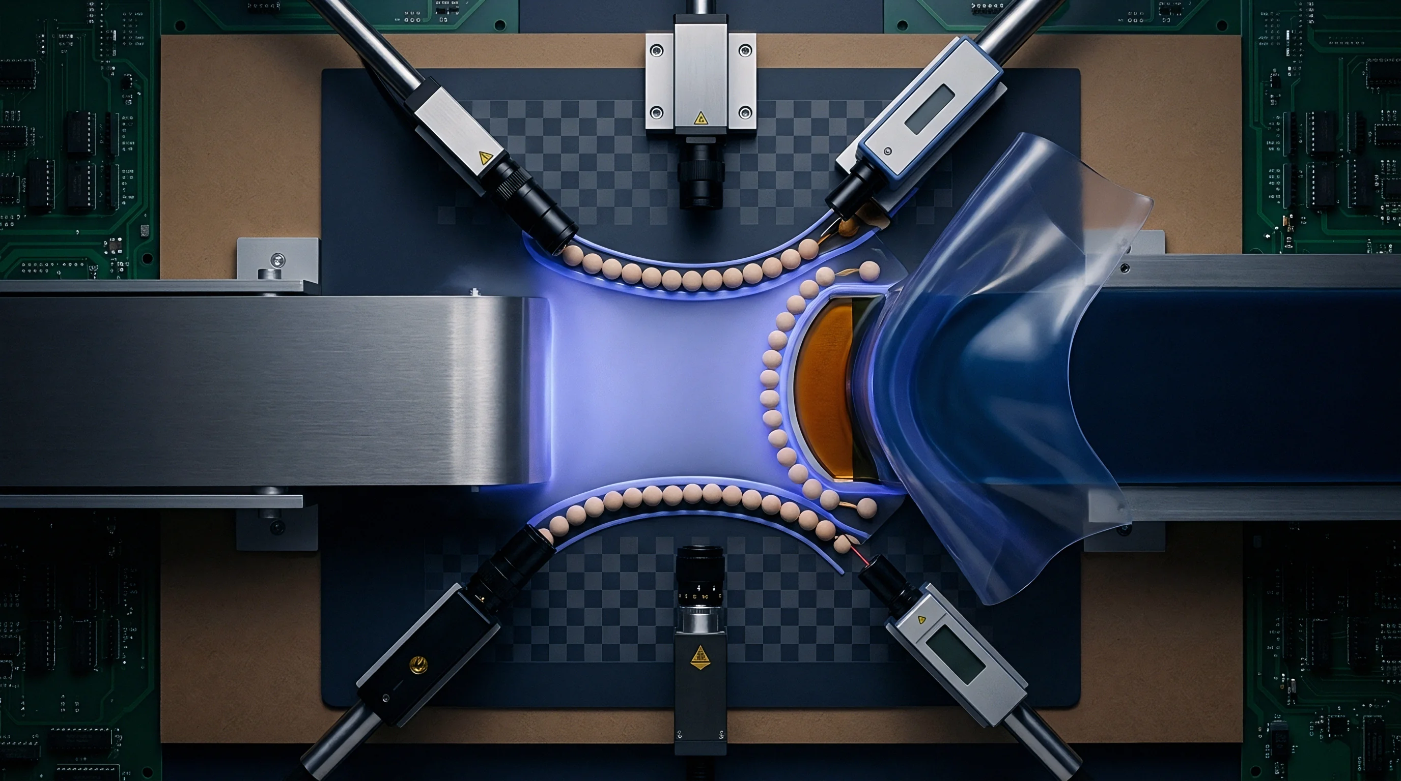
Rigorous dynamic qualification requires liquid-to-liquid thermal shock systems or rapid thermoelectric Peltier test stages capable of driving controlled thermal transitions exceeding 15 degrees Celsius per second. The sensor under test mounts to a specialized PCB fixture, exposed to rapid temperature changes while subjected to constant reference pneumatic pressures delivered through rigid, non-compliant stainless steel tubing. If the dynamic compensation algorithm functions correctly, digital output pressure remains flat within stated precision envelopes throughout rapid thermal shocks.
Algorithms lacking rate-of-change compensation produce pronounced transient spikes, often exceeding five to ten times steady-state error ratings during rapid temperature swings.
Dynamic thermal qualification demands temperature transitions faster than ten degrees Celsius per second while holding target pneumatic pressure steady within 0.05 hectopascals.
Dynamic test sequences require high-accuracy external reference transducers isolated from ambient thermal shocks. The reference pressure transducer sits in an externally controlled, temperature-stabilized enclosure, connected to the active pressure chamber through thermal delay tubes. This test layout guarantees that variations observed on the digital bus reflect mechanical package stress within the device under test rather than pneumatic source fluctuations.
Firmware developers log time-stamped raw pressure codes, raw temperature codes, and host-calculated compensated outputs alongside reference transducer telemetry at millisecond intervals.
This verification data reveals whether the dynamic compensation algorithm achieves the required transient rejection performance under realistic field environments. Tracking residual pressure errors across multiple thermal shock cycles confirms that viscoelastic relaxation constants and rate-dependent derivatives remain stable across wide operating ranges.
Whether prolonged exposure to high-frequency acoustic noise permanently degrades viscoelastic die-attach properties remains unresolved in published packaging studies.