Finite Element Prediction of Underfill Creep and Sensor Offset Drift
Finite element modeling of underfill viscoelastic creep enables precise prediction of die stress relaxation and dynamic digital offset drift in encapsulated sensors.
Finite element modeling of underfill viscoelastic creep enables precise prediction of die stress relaxation and dynamic digital offset drift in encapsulated sensors.
Interfacial shear lag concentrates thermal mismatch forces at package corners, requiring precise standoff height and pad geometry control to prevent joint fatigue.

Silicon thermal expansion mismatch induces mechanical packaging stresses that drive piezoresistive offset drift, requiring compliant anchors or ceramic mounts.

Common centroid geometry eliminates linear gradients in precision silicon references, transferring residual drift limits entirely to packaging stress and bus trim.

Wafer-level package shear mechanics rely on ball standoff height, pad geometry, and underfill to mitigate thermal expansion mismatch across solder joints.

Ductile metallic interlayers absorb anodic thermal contraction through plastic shear, cutting post-bond bow from 80 to under 20 micrometers on 150-millimeter stacks.

Intermetallic growth stiffens the solder substrate interface, converting creep strain into high interfacial shear stresses that accelerate thermal fatigue failure.
Calculate viscoelastic stress transfer by fitting multi-mode Prony series DMA data and applying Arrhenius-corrected shift factors under thermal cycling dwells.

Orthogonal cross-quad bipolar layout cancels linear packaging stress and inverts shear vectors to stabilize bandgap reference drift below two millivolts.

Thermal expansion mismatches in transducer packaging transfer mechanical stress to silicon dies, driving zero offset drift and signal hysteresis under thermal cycling.

Dynamic elasticity tensor tracking uses embedded piezoresistive rosettes and recursive inversion to cancel interposer viscoelastic warpage in real time.
Wafer-level package parasitic inductance variance shifts serial channel return loss and eye margins, requiring strict standoff height controls during assembly.

Viscoelastic mold compound relaxation during thermal cycling alters sensor die stress, causing unrecoverable analog drift unless modeled via Prony series.
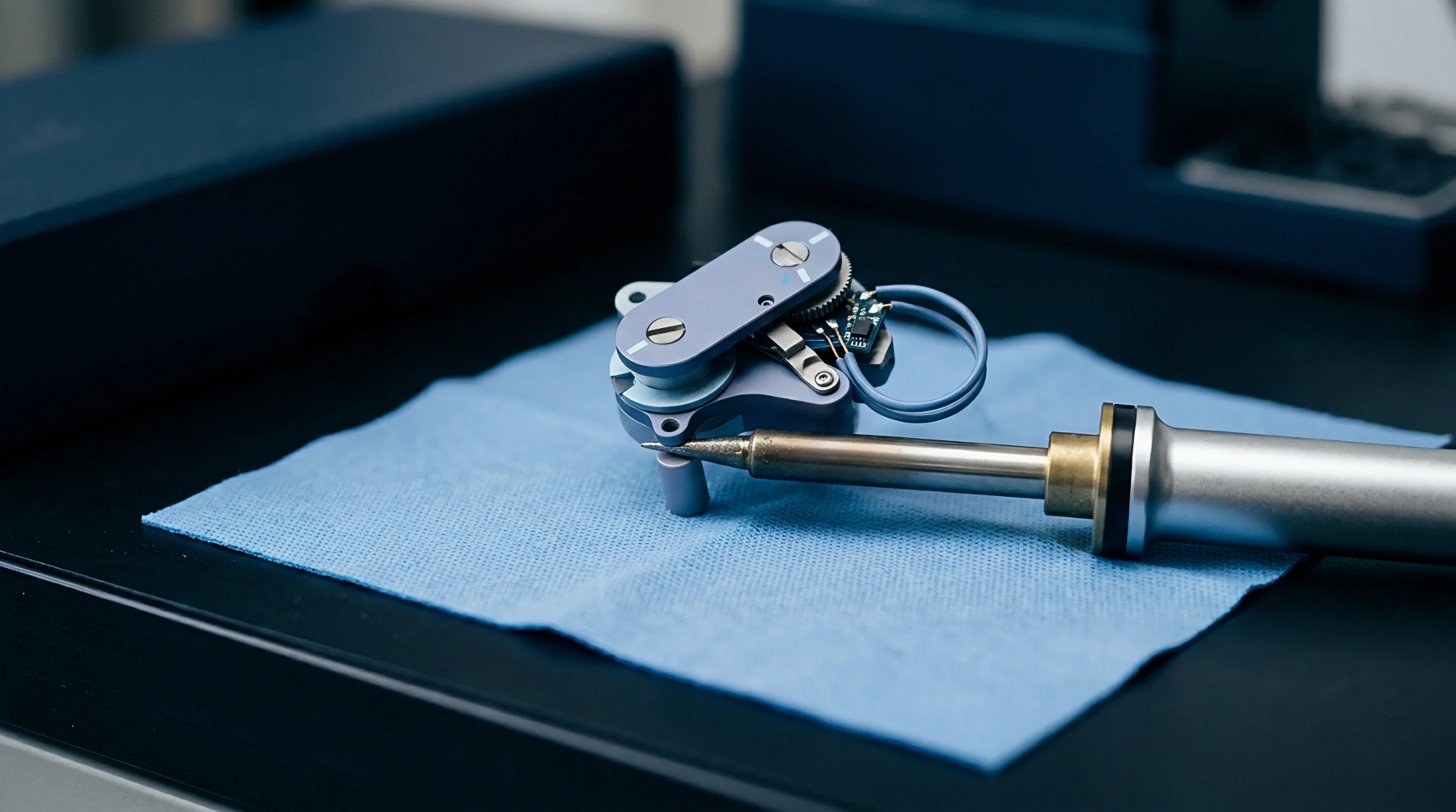
Thermal expansion mismatch in fine-pitch packages concentrates shear strain in outer joints, demanding matched underfill and strict standoff control to survive.

Unpassivated wafer conversion packaging transfers mold compound reflow stresses directly into analog trim circuits, shifting factory register offsets.

Mitigate high-modulus gel interfacial shear by combining silane-promoted substrate adhesion, laser stress relief trenches, and dual-layer modulus gradients.
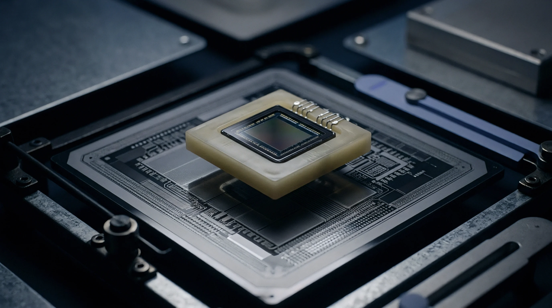
Eliminating protective mold compounds exposes silicon directly to board flexure and solder creep, driving piezoresistive offset shifts across temperature.

Ultra-thin wafer-level sensors lose flexural rigidity at sub-100 micrometer thicknesses, transferring solder and PCB viscoelastic creep directly into active sensing elements.
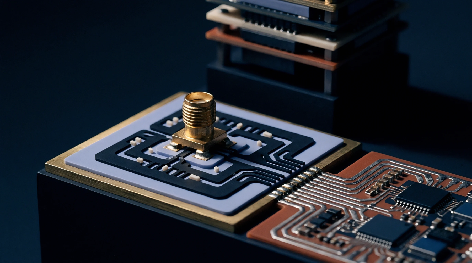
Determining clock low bounds across thermal cycles requires evaluating internal oscillator drift, package piezoresistive strain, and supply rail variations.
Factory-calibrated modules eliminate board-level thermal stress drift through mechanical decoupling and pre-programmed trim, justifying higher unit costs.

Cascade enable logic eliminates individual chip-select routing across dense sensor arrays by propagating a single hardware token down a shared serial bus.

Characterizing substrate interface viscoelastic shear relaxation prevents dynamic thermal offset drift and avoids expensive late stage packaging redraws.

Polymer viscoelastic stress relaxation in molded MEMS packages causes long-term zero-point offset drift that requires cavity isolation or baked burn-in.

Precision voltage reference accuracy depends on isolating packages from board flexure, balancing trace Seebeck junctions, and blocking thermal conduction paths.

Board flexure stress couples to analog dies via solder joints and mold compounds, shifting bandgap voltages up to 10 millivolts under thermal cycling.

Driving current from an analog sensor output heats internal silicon sub-circuits, creating thermal gradients that drift the internal voltage reference beyond nominal tolerances.
Expertise is a utility, not a secret. sentiention™ publishes its working knowledge as open reference: intelligence layer covering the materials it sources, the markets it enters, and the reference that serves both.