Substrate Interface Shear Stress Mitigation Strategies for High Modulus Gel Filled Sensor Assemblies
Mitigate high-modulus gel interfacial shear by combining silane-promoted substrate adhesion, laser stress relief trenches, and dual-layer modulus gradients.

Boundary
Sensor dies isolated by silicone gels experience zero shear stress under purely hydrostatic pressure fields. Mechanical shear originates at the boundary where the potting material meets the package housing, the passivated silicon surface, and the printed circuit board substrate. When a gel with a high storage modulus (G’ exceeding 50 kPa at 20 degrees Celsius) cures inside a rigid package well, thermal excursions force differential volumetric movements between the organic polymer and inorganic surfaces.
Silicon exhibits a coefficient of thermal expansion near 2.6 ppm per Kelvin. Substrate laminates such as FR-4 expand at 14 to 17 ppm per Kelvin in-plane. High-durometer potting compounds expand at 150 to 300 ppm per Kelvin.
This thermal expansion mismatch generates interfacial shear stresses exceeding 800 kPa at the die perimeter during standard automotive thermal cycles between -40 and 125 degrees Celsius.
The resulting boundary displacement couples directly into the active transduction zone. In piezoresistive pressure cells, die surface shear deforms the internal Wheatstone bridge resistors, introducing output span errors and baseline drift. Capacitive microelectromechanical systems register parasitical substrate deformation as false capacitance shifts.
The shear profile follows a steep gradient, maximizing at the peripheral corners of the die-attach plane while falling to zero at the geometric center of the die.
Peak interfacial shear stress scales linearly with the polymer’s shear modulus and the distance from the neutral point of thermal expansion.
Mitigation begins by controlling the modulus transition zone. Low-modulus gels (G’ between 0.5 and 5 kPa) absorb boundary displacement through bulk compliance, yet they fail under high-velocity media impact, aggressive fluid cavitation, and high fluid pressure heads. Assemblies operating in harsh environments adopt high-modulus gels (G’ between 50 and 500 kPa) or fluorosilicone gels to resist chemical extraction, fuel permeation, and mechanical wash-out.
This chemical resilience transfers the full mechanical burden of displacement onto the substrate interface. Designers resolve this tradeoff by altering the physical topology of the substrate, introducing compliant compliance barriers, or selecting stress-decoupling package footprints.
The land pattern and package outline govern the mechanical load delivered from the parent board into the gel chamber. A leadless Quad Flat No-Lead (QFN) or Land Grid Array (LGA) package solders directly to the mainboard, creating an intimate mechanical path for board warp to flex the package cavity floor. When the floor flexes, the high-modulus gel transmits this flexure directly to the die edges as secondary shear.
Leadframe packages featuring gull-wing leads (such as Small Outline Integrated Circuits) introduce mechanical compliance between the board and the housing, decoupling mainboard warp from the gel well. A leaded footprint reduces transferred package stress by roughly 70 percent compared to an LGA footprint of equivalent area.
Assembly line economics define the boundary of acceptable mitigation. Adding silicone compliant boots, secondary compliant underfills, or isolated sub-mount headers increases component height and extends the process bill of materials. The sourcing team balances the yield drop caused by interfacial shear failure against the added cycle time of dual-dispense cure lines.
An improper stress mitigation choice leaves the board assembly vulnerable to complete interfacial delamination during routine thermal shock testing.


Adhesion
Interfacial shear mitigation operates on two mechanical fronts: reducing the absolute shear load or raising the interfacial shear strength above the operating stress floor. Adhesion failures occur when interfacial shear stress exceeds the critical interfacial fracture toughness (G_ic) of the bonded surfaces. For silicone gels meeting passivated silicon nitride or polyimide coatings, G_ic values drop significantly if surface energy balances are poorly controlled prior to dispensing.
Surface Energy Modification Protocols
Bare printed circuit board substrates and ceramic carriers present heterogeneous surfaces composed of solder mask, copper pads, glass weave, and exposed dielectric resin. High-modulus potting compounds fail to wet these varied zones uniformly without targeted pre-treatment. Oxygen plasma cleaning and atmospheric pressure helium-oxygen plasma treatment increase substrate surface energy from baseline values of 32 to 38 dynes per centimeter up to 68 to 72 dynes per centimeter.
This energy shift promotes thermodynamic wetting, driving the contact angle of uncured silicone prepolymers below 15 degrees.
Chemical silane primers provide covalent bridging across the substrate-gel boundary. Methacryloxypropyltrimethoxysilane and glycidoxypropyltrimethoxysilane form siloxane bonds (Si-O-Si) with inorganic silica fillers, ceramic headers, and passivated die surfaces, while integrating into the silicone polymer network during platinum-catalyzed thermal curing. The table below compares the shear adhesion properties of common interface pairings evaluated under standard lap-shear configurations per ASTM D1002.
| Substrate Base Material | Surface Pre-Treatment | Contact Angle (Degrees) | Shear Adhesion (kPa) | Failure Mode |
|---|---|---|---|---|
| FR-4 High-Tg Epoxy Mask | None (As-Received Solvent Degreased) | 58 ± 4 | 140 ± 25 | Adhesive Delamination |
| FR-4 High-Tg Epoxy Mask | Oxygen Plasma (300 W, 120 s) | 14 ± 2 | 460 ± 40 | Mixed Adhesive/Cohesive |
| FR-4 High-Tg Epoxy Mask | Plasma + Organofunctional Silane | 8 ± 1 | 890 ± 60 | Cohesive Gel Rupture |
| Alumina Ceramic (Al2O3 96%) | Solvent Cleaned (IPA Ultrasonic) | 44 ± 3 | 220 ± 30 | Adhesive Delamination |
| Alumina Ceramic (Al2O3 96%) | Plasma + Organofunctional Silane | 6 ± 1 | 980 ± 50 | Cohesive Gel Rupture |
| Silicon Die (Si3N4 Passivated) | Solvent Cleaned (IPA Ultrasonic) | 38 ± 3 | 310 ± 35 | Adhesive Delamination |
| Silicon Die (Si3N4 Passivated) | Plasma + Organofunctional Silane | 5 ± 1 | 1120 ± 70 | Cohesive Gel Rupture |
Silane primers must cure under controlled relative humidity conditions between 40 and 60 percent. Moisture starvation during primer hydrolysis prevents silanol generation, cutting bond strength in half. Primers applied at excessive thicknesses (exceeding 0.5 micrometers) create a brittle, glassy interlayer that shears prematurely under low cyclic strain amplitudes.

Micro-Texturing and Mechanical Interlocking
Direct mechanical interlocking augments chemical adhesion. Laser direct structuring (LDS) or picosecond laser surface ablation creates micro-grooves and re-entrant pits within the substrate cavity floor. A trench pattern with pitch dimensions of 25 micrometers and depths of 10 micrometers traps the high-modulus elastomer, converting interfacial planar shear into compressive and tensile stress vectors distributed across three dimensions.
The geometry of the cavity wall where the gel terminates dictates peel stress generation. Sharp 90-degree internal corners at the cavity perimeter act as catastrophic stress risers. During thermal contraction, the gel meniscus pulls inward, initiating cohesive tears at the cavity lip.
Machining or molding the cavity with an internal draft angle between 7 and 12 degrees reduces boundary notch factors, distributing interfacial shear stress across a broader surface area.
Substrates running copper pad transitions within the gel well require special copper finish selection. Electroless Nickel Immersion Gold (ENIG) exhibits stable bonding with silane-modified silicones. Immersion Tin (ImSn) surfaces develop intermetallic compound (IMC) growth that can alter local surface stiffness and promote micro-voiding beneath the gel boundary over long operating lifetimes at elevated temperatures.
Applying silane chemistry without continuous atmospheric humidity control yields unpredictable bond cohesion across high-volume production lots.

Trench
When chemical bonding alone cannot arrest shear forces, packaging engineers incorporate mechanical isolation features into the package cavity floor. Stress relief trenches cut the continuity of the displacement vector running from the peripheral package walls to the active sensor footprint. These micro-machined, molded, or routed features alter the mechanical compliance of the substrate plane surrounding the silicon die.

Perimeter Stress Grooves and Kerfs
A perimeter trench surrounding the die footprint isolates thermal strain. As the high-modulus gel expands during reflow or elevated temperature exposure, the expanding mass within the trench moves independently from the mass resting over the active sensor center. The presence of an open trench acts as an expansion reservoir, converting horizontal shear displacement into vertical gel swelling.
Trench depth determines mechanical isolation efficiency. Finite element modeling and empirical cross-sectioning indicate that trench depth must equal at least 60 percent of the die thickness to decouple substrate strains effectively. In multilayer low-temperature co-fired ceramic (LTCC) or high-density interconnect (HDI) organic substrates, these trenches are produced during laser routing stages before surface mount placement.
- Mechanical Routing cuts perimeter channels with endmills down to 200 micrometers in diameter, delivering vertical trench walls with a positional tolerance of ±25 micrometers across the substrate panel.
- Laser Cavity Ablation utilizes ultraviolet picosecond lasers to carve trenches with widths down to 50 micrometers, avoiding micro-cracking in sensitive ceramic substrates.
- Secondary Step Etching creates tiered shelf geometries within the cavity floor, establishing multi-stage shear dampening regions adjacent to the die perimeter.
- Controlled Solder Mask Dams build elevated perimeter barriers (25 to 40 micrometers tall) that block the horizontal propagation of high-modulus gel layers directly beneath the die edges.
Deep relief trenches convert lateral thermal shear into unconstrained vertical displacement along the open gel boundary.
Substrate routing introduces venting challenges during high-modulus gel dispensing. Deep, narrow trenches trap micro-bubbles of ambient air. These air voids alter local thermal conductivity and collapse under high operating pressures, producing localized pressure drops that degrade measurement accuracy.
Vacuum dispensing at chamber pressures below 50 mbar eliminates trapped gas pockets within high-aspect-ratio relief trenches.

Pedestal Mounts and Sub-Mount Decoupling
Elevating the sensor die above the cavity floor on a silicon or ceramic sub-mount isolates the die from interfacial shear stresses. The sub-mount functions as an intermediate platform matching the thermal expansion coefficient of the sensor element (2.6 to 4.0 ppm per Kelvin). The high-modulus gel envelops the sub-mount perimeter, but the lateral shear strains generated along the package floor terminate at the sub-mount base rather than the active die surface.
Sub-mount attachment demands die-attach adhesives with low elastic moduli. A soft silicone or modified epoxy die-attach with a modulus below 10 MPa absorbs shear displacement transmitted from the package floor. The thickness of this bondline governs stress transfer.
Bondlines thinner than 30 micrometers transmit excessive shear strain; bondlines held between 50 and 80 micrometers provide optimum isolation without introducing die tilt or angular placement errors that impair wire-bonding yields.
Neglecting vacuum assist during the dispensing of high-modulus potting compounds over deep trenches generates air pockets that induce sensor hysteresis under pressure cycling.

Stack
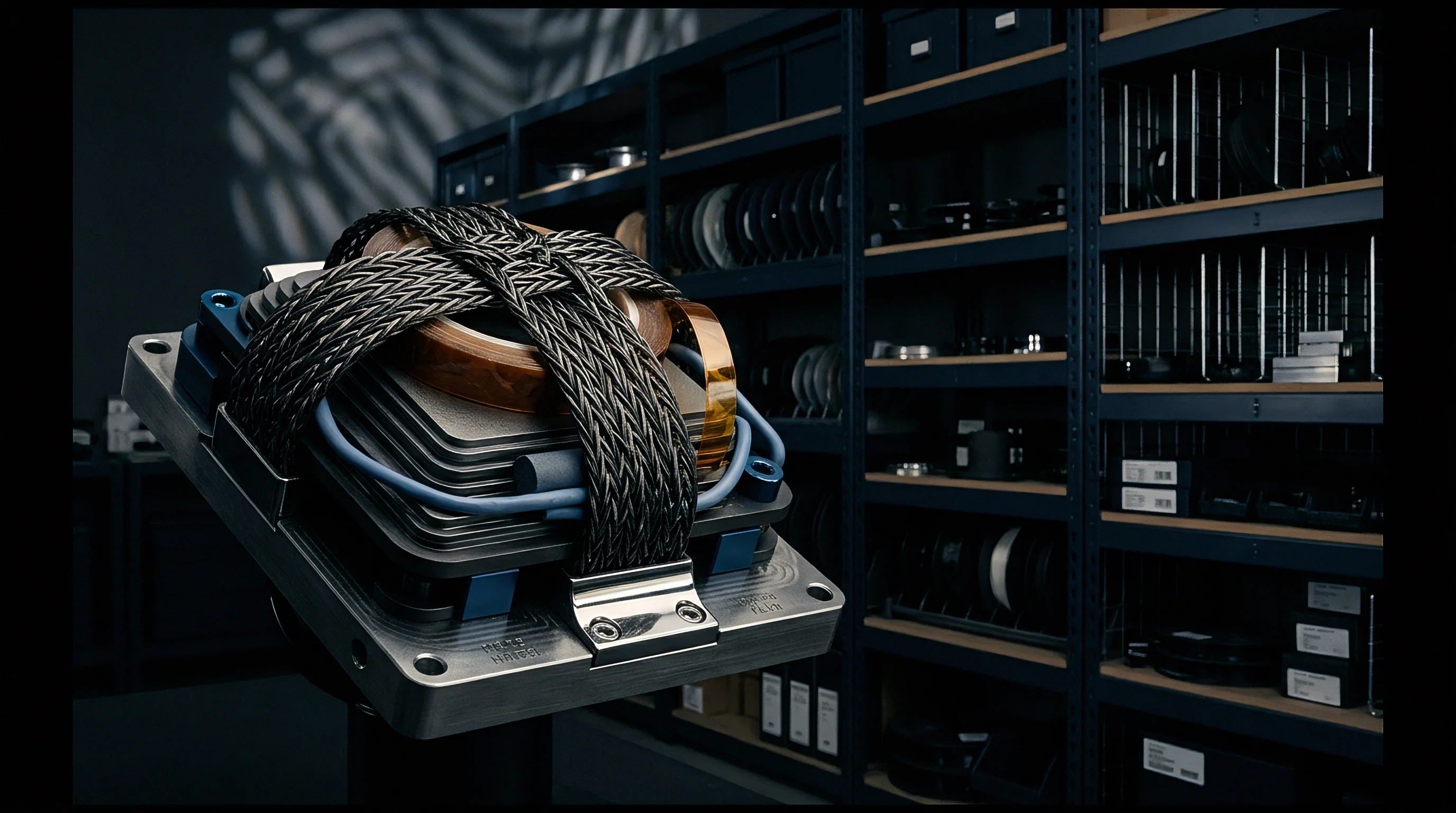
A single potting material rarely satisfies both media compatibility and mechanical decoupling criteria. Multi-layer potting architectures deploy gradient modulus structures. A primary, ultra-soft silicone layer coats the die surface and interfacial substrate zones.
A secondary, high-modulus, media-resistant gel covers the soft base layer, sealing the assembly against automotive fluids, sour gas, or high-pressure steam.
Modulus Gradient Architecture
Dual-layer gel stacks decouple the transduction zone from harsh external environments. The primary gel layer, dispensed to a controlled height just covering the active die surface and wire bonds, exhibits a shear modulus between 0.5 and 2.0 kPa. The secondary capping gel possesses a shear modulus between 80 and 300 kPa.
The low-modulus base layer deforms under minimal stress, absorbing any displacement from package floor expansion or mainboard warp. The high-modulus top layer acts as a flexible, impervious membrane.
The capping gel must bond chemically to the base layer to prevent internal delamination. Silicone chemistries using identical platinum catalyst systems (addition-cure hydrosilylation) cross-link across the liquid-liquid or liquid-gel interface when cured sequentially. If the primary layer is cured to full conversion before secondary dispensing, unreacted vinyl groups become scarce, weakening interlayer adhesion.
Controlled B-stage curing of the base layer (heating to 80 degrees Celsius for 15 minutes to reach roughly 70 percent conversion) preserves active chemical sites, establishing a seamless mechanical gradient.
| Layer Configuration | Base Layer Modulus G’ | Cap Layer Modulus G’ | Die Surface Shear (kPa) | Media Swell In Hexane (%) |
|---|---|---|---|---|
| Single Layer Standard Gel | 2.5 kPa | None | 12 ± 2 | 42 ± 5 |
| Single Layer High-Modulus Gel | 180 kPa | None | 620 ± 45 | 4 ± 1 |
| Single Layer Fluorosilicone | 95 kPa | None | 380 ± 30 | 1.5 ± 0.5 |
| Dual Layer (Soft Gel + High G’ Cap) | 1.8 kPa | 210 kPa | 24 ± 4 | 3.8 ± 0.8 |
| Dual Layer (Soft Gel + Fluorosilicone) | 1.8 kPa | 95 kPa | 18 ± 3 | 1.2 ± 0.3 |
Layer thickness ratios alter the mechanical transmission of external loads. A base layer thickness less than 150 micrometers over the die surface permits the stiff capping layer to mechanically compress the bond wires during low-temperature contraction. Maintaining a minimum base layer clearance of 300 ± 50 micrometers above the die and wire-bond loops protects the electrical interconnections from fatigue-induced fracture.

How Do Modulus Gradients Shift under Thermal Aging?
Continuous thermal exposure alters the polymeric network through post-curing and thermal oxidation. When operated above 150 degrees Celsius, standard dimethylsilicone gels undergo chain scission and cross-linking reactions. The storage modulus of a 2.0 kPa base gel can rise to 15 kPa over 1,000 hours of continuous dwell at 150 degrees Celsius, increasing interfacial shear stress by a factor of seven.
Phenyl-modified silicones and fluoroalkylsilicones limit oxidative cross-linking, stabilizing the modulus curve across extended operational spans.
Fluid absorption also modifies the stress state of the stack. Non-polar solvents and automotive fuels permeate high-modulus silicone layers, inducing volumetric swelling. Swelling creates an internal compressive hydrostatic stress state combined with high interfacial shear at anchored edges.
Fluorosilicone capping gels with trifluoropropyl side groups prevent hydrocarbon absorption, maintaining volumetric stability and holding swell-induced shear below 50 kPa under complete fluid immersion.
Incompatible cure chemistry between the base gel and the cap gel leads to unreacted platinum inhibition, leaving an uncured liquid interface that shifts calibration points under vibration.


Yield
Stress mitigation strategies alter manufacturing throughput and final testing yields. Packaging choices that eliminate interfacial shear on the bench can introduce process liabilities that depress line yields during automated assembly. A sensor package must survive high-speed pick-and-place, automated optical inspection, standard reflow profiles, fluid dispensing, and thermal calibration cycles without accumulating latent defects.

Process Complexities and Cycle Times
Dual-gel dispensing operations demand two dedicated precision valve systems and staged curing ovens. A single-gel dispense cycle takes roughly 3.5 seconds per component. A dual-gel architecture requires dispensing the base layer, a 15-minute intermediate flash cure, a second dispense cycle for the capping gel, and a final 60-minute thermal cure.
This sequence expands capital expenditure on curing infrastructure and increases work-in-progress inventory along the surface-mount assembly line.
Underfill dispensing beneath sub-mounts or leadless package carriers presents another process constraint. Capillary flow under large-die packages requires heated stages (70 to 90 degrees Celsius) and tight dispense weight tolerances (±1.5 milligrams). Incomplete underfill filleting creates voiding at package corners, concentrating thermal expansion forces and driving localized solder-joint fatigue during subsequent reflow sweeps.
Yield loss also tracks wire-bond integrity during high-modulus gel injection. The dynamic viscosity of high-modulus formulations (often exceeding 8,000 mPa·s prior to cross-linking) exerts viscous drag on gold or aluminum bond wires during high-speed potting. Wire sweep exceeding 3 percent of wire length risks electrical shorts between adjacent lines or neck-down fractures at the heel of the wedge or ball bond.
Lowering dispense dispense rates or tilting dispense needles reduces incoming fluid velocity, limiting wire displacement at the expense of cycle time.
Wire sweep during viscous potting increases exponentially when the gel dispense velocity exceeds ten millimeters per second.

Digital Compensation against Residual Stress
Hardware isolation techniques rarely eliminate interfacial stress entirely. Residual shear stresses manifest as predictable temperature-dependent offset drift and span shifts. Modern sensor packaging lines integrate digital signal conditioning ASICs (Application-Specific Integrated Circuits) directly within the package or adjacent to the sensor well to calibrate out these repeatable mechanical effects.
- Multi-Point Temperature Calibration maps sensor output across five discrete thermal targets, storing second-order polynomial compensation coefficients in on-chip EEPROM.
- Integrated Piezoresistive Stress Sensors embedded directly in non-active corners of the silicon die monitor in-situ substrate stress, providing a direct hardware input to the ASIC compensation algorithm.
- Digital Bus Communication over standard I2C, SPI, or SENT (Single Edge Nibble Transmission) interfaces transmits compensated data directly to host ECUs, masking residual baseline shifts from the application controller.
- Programmable DSP Filters smooth transient response artifacts generated when sudden thermal shocks cause instantaneous gel expansion before mechanical equilibrium is restored.
Calibrating each part across multiple thermal dwell points drives substantial line costs. A two-point calibration routine requires 45 seconds of bench test time per unit. A five-point calibration sweeps parts through thermal test chambers over 20 minutes, demanding high-density parallel test sockets.
When sourcing sensor modules, buyers weigh the cost of complex physical isolation (such as sub-mounts and relief trenches) against the operational test cost of extensive digital calibration routines.
Skipping thermal calibration to lower unit costs transfers mechanical offset errors directly into the host controller, triggering field recalibration faults.
Settlement
Evaluating stress mitigation mechanisms culminates in the total landed cost of the sensing system. Sourcing teams encounter five distinct component form factors for a given silicon sensing die: bare die, surface-mount leadless (LGA/QFN), surface-mount leaded (SOIC), embedded header module, and fully integrated standalone cabled probe. Each package iteration shifts mechanical isolation burdens between the component vendor, the board assembly contractor, and the host system integrator.

Total Landed Cost across Package Variants
Bare die procurement yields the lowest component purchase price but demands high cleanroom investment, automated die-attach equipment, wire bonders, precision dispensing lines, and dedicated calibration ovens. Purchasing a fully packaged LGA or QFN pressure sensor shifts the wire bonding and cavity potting to the tier-one semiconductor packaging house. However, the buyer remains responsible for managing board-level shear transfer, requiring strict land pattern control, compliant solders, or soft potting underfills on the mainboard.
Standalone cabled probes house the die inside a stainless steel or brass housing, isolated by soft oil-filled diaphragms or multi-layer potting assemblies. The probe vendor absorbs the calibration and stress mitigation costs entirely, delivering a calibrated linear analog or digital output to the customer. This mechanical isolation raises component procurement costs by an order of magnitude.
The table below outlines typical commercial and assembly parameters for a standard 10-bar automotive media-isolated pressure sensor element delivered across five package configurations.
| Package Variant | Unit Cost (10k pcs) | Board Area (mm²) | Integration Overhead | Typical Yield (%) | Host Bus Format |
|---|---|---|---|---|---|
| Bare Silicon Die | $1.85 ± $0.15 | 4.2 ± 0.2 | Cleanroom Wire Bond + Gel Line | 91.5 ± 2.0 | Raw Bridge (Analog) |
| SMD LGA (Leadless) | $3.90 ± $0.25 | 25.0 ± 1.0 | Standard SMT + Underfill Option | 98.2 ± 0.5 | I2C / SPI / Analog |
| SMD SOIC-16 (Leaded) | $4.85 ± $0.30 | 110.0 ± 5.0 | Standard SMT Assembly | 99.4 ± 0.3 | I2C / SPI / SENT |
| Embedded Header Module | $8.50 ± $0.60 | 180.0 ± 10.0 | Through-Hole Solder / Press-Fit | 99.6 ± 0.2 | SENT / LIN / Analog |
| Housed Cabled Probe | $24.50 ± $1.80 | Cabled Remote | Mechanical Bracket + Wiring Harness | 99.9 ± 0.1 | CAN / LIN / 4-20mA |
Minimum order quantities (MOQs) mirror these manufacturing tiers. Standard leadless LGA components distribute through global supply channels with reel sizes of 2,500 or 5,000 units, supporting low-volume prototyping. Customized embedded header modules with proprietary gel stacks or laser-trenched substrates carry factory MOQs of 20,000 to 50,000 pieces due to custom tooling, mold inserts, and dedicated dispenser setup requirements.
Tooling charges for specialized header molds run between $40,000 and $120,000, presenting a notable upfront capital barrier.

Make versus Buy Arithmetic
To identify the economic tipping point between mounting bare elements into an in-house potted cavity versus purchasing pre-packaged and pre-calibrated sensor units, engineering and finance teams model the fully burdened manufacturing cost. Assume an annual demand of 100,000 units. The fully packaged SOIC-16 variant with an internal compliance layer costs $4.85 per unit, totaling $485,000 in direct bill-of-materials spend.
SMT assembly adds $0.08 per placement, and basic single-point post-assembly functional testing costs $0.12 per board, producing an integrated landed cost of $5.05 per placed sensor.
Building the sensor in-house using bare die elements ($1.85) mounted into an injection-molded housing ($0.45) requires die-attach adhesive ($0.05), wire bonding ($0.18), dual-layer gel dispensing ($0.32), and two-stage thermal cure oven cycles ($0.14). Line yield losses of 8.5 percent add $0.27 per functional part. Five-point thermal calibration on automated testing nests costs $1.45 per unit when accounting for equipment depreciation, cycle time, and direct labor.
The in-house assembly landed cost totals $4.71 per unit. At 100,000 units annually, the in-house assembly pathway generates $34,000 in gross operational savings.
However, amortizing the $180,000 capital expense of an automated dual-fluid dispenser, a plasma surface cleaner, and a multi-chamber thermal calibration handler over three years introduces a yearly depreciation load of $60,000. Under these baseline assumptions, the in-house manufacturing strategy incurs a net annual loss of $26,000 compared to purchasing the pre-calibrated SOIC-16 package. The make-or-buy break-even threshold flips in favor of in-house manufacturing only when production volumes exceed 280,000 units annually, where the fixed calibration depreciation is distributed over a broader unit base.
Component buyers must inspect vendor qualification dossiers for thermal cycling compliance. Standard testing mandates 1,000 cycles from -40 to 125 degrees Celsius per JEDEC JESD22-A104. When a supplier substitutes a lower-cost, higher-modulus gel without adjusting the underlying substrate stress relief trenching, the buyer enforces a warranty reserve adjustment or rejects the bill of materials change outright.
Standard purchase contracts stipulate that any unannounced alteration of potting gel durometer, base-layer fill height, or cavity surface treatment constitutes a breach of specification, obligating the vendor to reimburse all associated recall and board scrap expenses.