Wafer Level Package Strain Transfer Mechanics and Land Patterns
Board strain transfers directly into wafer-level dies, requiring NSMD pads, stress isolation routing, or underfill to prevent fatigue and analog drift.


Anchor

Die Mechanics under Board Warpage
Wafer-level chip scale packages eliminate the intermediate organic substrate, placing monocrystalline silicon directly above the printed circuit board through an array of solder interconnects. Silicon exhibits an isotropic thermal expansion coefficient near 2.6 parts per million per Kelvin. Standard FR4 laminate expands at 14 to 17 parts per million per Kelvin in the in-plane axes.
The entire thermal and mechanical displacement gradient between the system board and the semiconductor core concentrates across the stand-off height of the solder joint. This mechanical coupling transfers board-level flexure directly into the active circuit face, altering transistor transconductance and sensor bridge balance through the piezoresistive effect.
A package without an interposer lacks mechanical compliance. When an external bending moment flexes the system board, the displacement vector travels through copper lands, solder bumps, and thin-film redistribution layers into the die bulk. The standoff height of an un-underfilled wafer-level package rarely exceeds 0.200 millimeters, leaving minimal volume for shear relaxation.
This unmediated path turns standard board handling, depaneling, and thermal cycling into immediate threats to electrical offset stability and structural interconnect integrity.
Underfill selection sets the shear plane position between the laminate substrate and the fragile silicon redistribution passivation.
Board deflection induces biaxial strain fields across the die surface. The active surface contains piezoresistors, reference amplifiers, or micro-electro-mechanical membranes that register mechanical stress as signal shift. A board warpage of 0.5 percent across a 50-millimeter span introduces localized stresses exceeding 70 megapascals in outer bump columns.
These stress levels disrupt sensitive analog calibration trims, shifting zero-g bias in accelerometers or offset voltages in bandgap references.
The routing density of the system board dictates the initial mechanical boundary condition. Thick copper planes on outer board layers increase local board stiffness, concentrating bending moments directly beneath the package perimeter. Designers often neglect the spatial relationship between inner-layer copper distribution and die strain transfer.
Balancing copper distribution balances the mechanical neutral axis of the assembled board assembly.
Solder joint geometry governs the transmission ratio of this mechanical energy. A barrel-shaped joint distributes shear evenly across its bulk. An hourglass joint concentrates stress at the narrower neck, accelerating fatigue cracking.
Controlling the land pattern geometry on the board side offers the primary design variable for shaping this joint profile, altering the transmission of board strains into the die.
The mechanical assembly tolerates elastic deformation until shear stresses reach the yield limit of the joint metallurgy. Beyond this threshold, plastic work accumulates with each thermal excursion. Unrelieved plastic strain terminates in solder crack propagation, redistribution metal rupture, or silicon substrate cracking known as package trace fracture.


Creep

Interconnect Viscoplasticity and Stress Relaxation
Solder joints operating near room temperature exist at high homologous temperatures, typically exceeding 0.65 of their absolute melting points. Under these operating environments, lead-free alloys such as SAC305 undergo continuous viscoplastic flow and creep deformation. The constitutive relationship governing this behavior is defined by the Anand viscoplastic model, which expresses the plastic strain rate through the equation:
dε/dt = A exp(-Q / (R T)) ^(1/m)
Here, dε/dt represents the inelastic strain rate, A is the pre-exponential factor, Q denotes activation energy, R defines the universal gas constant, T is absolute temperature, σ represents equivalent stress, s functions as the internal deformation resistance state variable, ξ scales stress, and m acts as the strain rate sensitivity exponent. At elevated assembly operational temperatures, solder creeps under sustained strains, relaxing overall package stresses over time while causing structural displacement drift.
Stress relaxation alters analog sensor precision over operating hours. When a board-mounted sensor undergoes heat exposure, board warpage shifts initial bump stress. As the solder creeps, mechanical stress relaxes non-linearly.
The silicon surface senses this variable stress via piezoresistive coefficients, producing an analog output drift entirely independent of environmental sensor variables. The sensor output shifts as the solder flows.
| Parameter | Symbol | Value | Unit |
|---|---|---|---|
| Pre-exponential Factor | A | 4.0 × 10^6 | 1/s |
| Activation Energy | Q / R | 9.4 × 10^3 | K |
| Stress Multiplier | ξ | 1.5 | dimensionless |
| Strain Rate Sensitivity | m | 0.30 | dimensionless |
| Hardening Constant | h0 | 1.8 × 10^5 | MPa |
| Deformation Resistance Saturation | s_sat | 2.5 × 10^1 | MPa |
The rate of stress relaxation is tied directly to joint stand-off height. Larger bump heights lower the shear strain range across the interconnect. Designers achieve increased stand-off through precise pad geometry selection.
Decreasing board pad diameters raises the liquid solder column during reflow, lifting the die and lowering steady-state plastic strain rates throughout field operation.
Thermal excursions induce continuous state-variable hardening followed by dynamic recovery within the bulk solder. In thermal cycling tests between negative 40 degrees Celsius and 125 degrees Celsius, cyclic shear strains induce recrystallization along grain boundaries. This microstructural coarsening concentrates strain along localized shear bands, precipitating early joint fatigue.
A solder joint operating above half its homologous melting temperature relaxes strain through steady-state atomic creep.
The time constant for complete mechanical stress relaxation varies widely across solder alloys. SAC305 relaxes the majority of peak installation stresses within 120 hours at 25 degrees Celsius. In harsh automotive applications subject to continuous vibration, external mechanical excitation superimposes dynamic fatigue over this static relaxation curve, accelerating microcrack formation near the die redistribution metallization interface.
A supplier can explain this shift by claiming factory calibration drifted under moisture exposure, obscuring the mechanical settling of the interconnect.


Land

Non-Solder-Mask Defined versus Mask-Defined Layouts
Land pattern geometry directly establishes the mechanical boundary conditions of the interconnect. Designers choose between Non-Solder-Mask Defined pads and Solder-Mask Defined pads. Non-Solder-Mask Defined pads feature copper lands etched smaller than the solder mask opening, exposing the copper side walls to molten solder during reflow.
Solder-Mask Defined pads feature solder mask overlapping the perimeter of a larger copper land, restricting wetting to the top horizontal copper plane.
Non-Solder-Mask Defined pads provide superior fatigue life during thermal cycling. Molten solder wets around the vertical edges of the copper land, anchoring the joint and distributing shear forces across a three-dimensional surface. This wetting profile eliminates sharp stress concentrations at the pad perimeter.
The resulting standoff height increases, reducing the total shear strain imparted to the low-k dielectric layers within the silicon die.
Solder-Mask Defined pads offer distinct advantages under board drop and high-strain mechanical bending tests. The broader copper trace anchored beneath the solder mask resists laminate tearing and pad cratering during dynamic shock events. Mask-defined pads create a rigid mechanical joint that concentrates shear strain at the solder-to-mask boundary, elevating crack propagation rates through the bulk solder during long-term thermal cycling.
| Design Feature | NSMD Dimension (mm) | SMD Dimension (mm) | Process Tolerance (mm) |
|---|---|---|---|
| Copper Pad Diameter | 0.200 | 0.280 | ±0.015 |
| Solder Mask Opening | 0.275 | 0.200 | ±0.025 |
| Solder Mask Clearance Web | 0.075 | 0.060 | ±0.010 |
| Target Standoff Height | 0.180 | 0.155 | ±0.020 |
| Solder Ball Diameter | 0.250 | 0.250 | ±0.010 |
The choice between these two land topologies defines the exact mechanical failure mode of the finished assembly. Solder-Mask Defined patterns transfer maximum stress into the fragile silicon passivation layers, occasionally leading to die fracture during board flex. Non-Solder-Mask patterns transfer mechanical loads into the laminate copper interface, trading dielectric risk for potential trace lifting on low-cost boards.
IPC-7351 guidelines specify design margins that must accommodate fabricator tolerances. Registration errors between copper imaging and mask exposure shift the solder bump alignment. If mask registration shifts by 0.025 millimeters on a fine-pitch pad, asymmetric wetting forces the package to twist, generating uneven residual stresses across the package perimeter upon solidification.
Fine-pitch designs at 0.35 millimeter and 0.40 millimeter pitch challenge standard liquid photoimageable solder mask resolution. Solder mask dams below 0.060 millimeters break down during board fabrication, causing solder bridging between adjacent pads. Designers must verify that the chosen printed circuit board vendor reliably resolves 0.050 millimeter solder mask webs before committing to high-density Non-Solder-Mask Defined layouts.
Adopting mismatched land pattern definitions produces asymmetric solder joints with disparate mechanical compliance across the array. The board designer ensures identical pad configurations across all package pins to prevent uneven tilting of the die surface during reflow cooling.

Trench

Stress Isolation Routing and Mechanical Relief
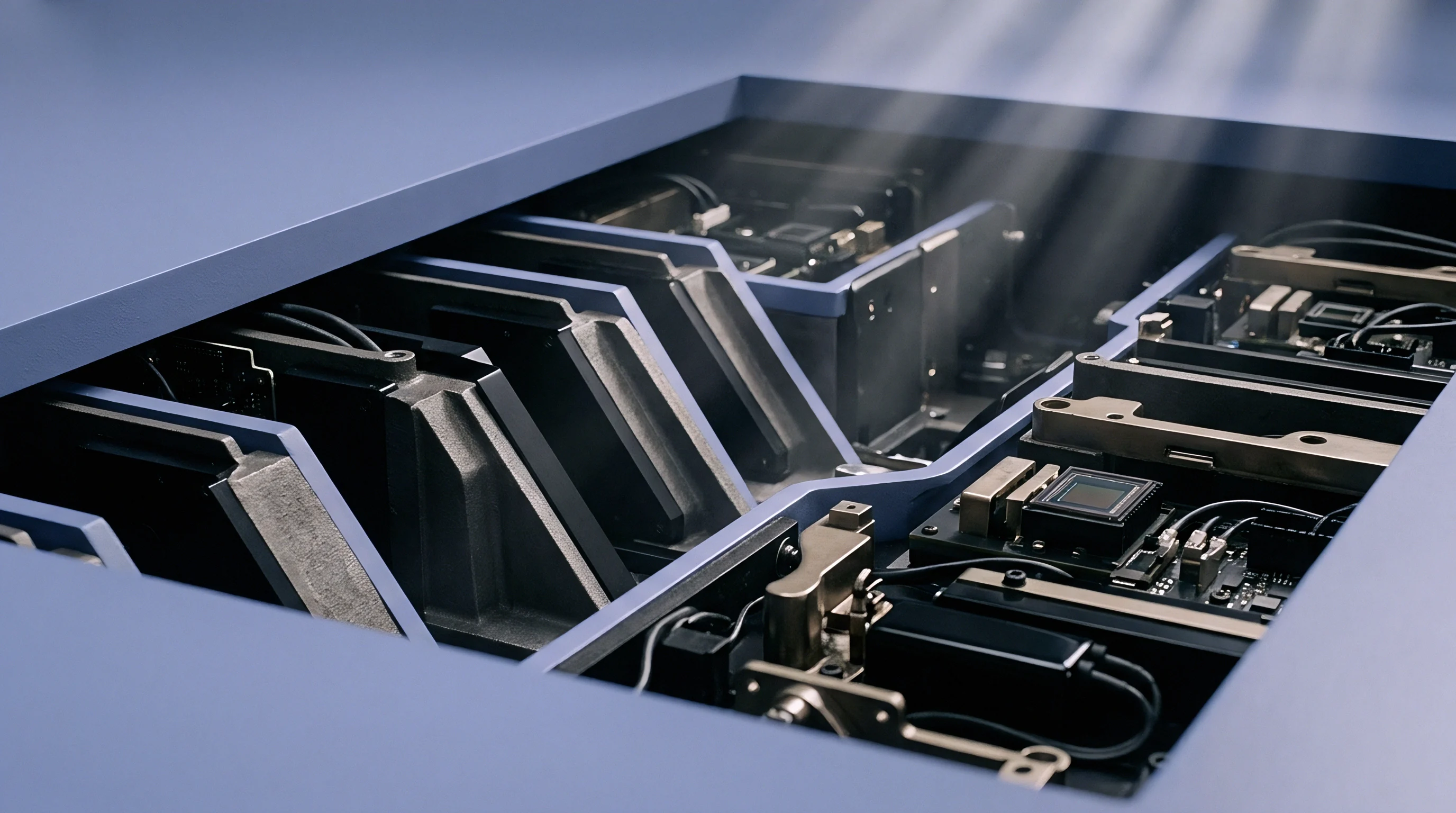
Circuit board flexure originates from chassis mounting points, connector insertions, and button actuations. These external loads travel across the laminate as flexural waves and static bend strains. Routing isolation slots, milling perimeter trenches, and punching mechanical relief cutouts directly into the circuit board breaks the continuity of the laminate, diverting bending strains around sensitive packages.
Isolating a wafer-level package requires thoughtful geometry. Placing an unbroken milled trench parallel to the long edge of the die interrupts the transverse strain path. The trench forces the mechanical neutral axis of the board to displace away from the package site, reducing localized surface strains by up to 70 percent under three-point bending loads.
The trench width must accommodate routing bit tolerances, typically requiring a minimum channel of 0.80 millimeters.
Board cutouts introduce routing restrictions that penalize signal path density. High-speed digital lines or sensitive analog sensor traces cannot traverse the physical air gap created by an isolation trench, forcing routing paths through narrow bridges of laminate. These structural bridges focus residual mechanical stress.
Placing critical traces across these bridges subjects the copper to elevated fatigue cycles during board vibration.
Alternative structural defenses preserve continuous laminate while mitigating strain transfer. Micro-perforated drill patterns, perimeter guard rings of unstrained dummy balls, and strategic placement near zero-moment inflection points provide substantial isolation without requiring through-hole routing slots. Designers keep wafer-level packages away from mounting screws, board edges, and heavy through-hole components such as inductors or connectors.
IPC-A-610 Class 3 inspection criteria reject assemblies exhibiting solder microcracks extending past twenty-five percent of the joint cross-section.
Component orientation relative to the principal board bending axis determines survival rates. Silicon dies are rectangular, with the long axis exhibiting significantly higher mechanical vulnerability to flexure than the short axis. Aligning the package so that its short axis parallels the primary board bend axis lowers peak tensile stress across corner solder joints, dampening strain transfer into the die circuitry.
Mechanical stiffeners placed on the opposing board side restrict local curvature. Bonding a passive stiffener or rigid steel plate beneath the package location prevents laminate bending beneath the bumps. The stiffener bonding adhesive introduces its own thermal expansion mismatch, demanding careful material characterization to prevent warpage over broad temperature ranges.
The ultimate efficacy of perimeter slotting depends entirely on systematic board edge constraints. An isolation scheme optimized for chassis twist may degrade drop shock performance if the milled trench allows the board to flutter uncontrollably upon impact, causing corner bumps to fail under excessive dynamic peeling moments.

Shift

Analog Drift versus Digital Bus Performance
Mechanical strain impacts integrated circuits through distinct physical mechanisms depending on whether the affected circuitry is analog or digital. Analog sensor cores and precision voltage references rely on matched differential pairs, current mirrors, and precision resistors. The piezoresistive effect shifts the resistivity of p-doped and n-doped silicon regions unevenly under anisotropic stress.
In contrast, digital circuits utilize complementary metal-oxide-semiconductor logic gates where stress merely alters carrier mobility without compromising Boolean state transitions.
Precision analog front ends, such as those found in factory-calibrated pressure sensors and three-axis accelerometers, experience significant baseline shift when subjected to package strain. Silicon piezoresistance coefficients for p-type silicon along the crystal orientation reach 71.8 × 10^-11 square meters per newton. A modest package-induced stress of 20 megapascals alters matched resistor networks by 0.14 percent, driving high-gain instrumentation amplifiers into severe DC offset drift and degrading factory calibration accuracy.
Digital interfaces, specifically Inter-Integrated Circuit and Serial Peripheral Interface lines, exhibit exceptional immunity to direct silicon strain. Carrier mobility fluctuations induced by package stress slightly adjust transistor drive currents, altering propagation delays by mere picoseconds. In typical 400-kilohertz I2C or 20-megahertz SPI protocols, these sub-nanosecond timing variations represent an insignificant fraction of the overall bit period, leaving bus integrity completely unaffected by mechanical flexure.
Digital communication over stressed interfaces degrades through structural interconnect failure rather than silicon performance shifts. Board flexure causes microcracking in solder bumps assigned to bus lines. An intermittent open circuit on the I2C serial data line corrupts the bus transaction, triggering bus stalls and software lockups that firmware developers mistake for timing violations or protocol errors.
The digital signal path fails catastrophically rather than drifting analog values.
Mitigating analog drift requires active layout compensation inside the die. Integrated differential sensor bridges incorporate cross-quad layout geometries that average out linear mechanical stress gradients across the die plane. Dummy redistribution bumps placed on the die periphery absorb the bulk of the package shear strain, shielding the sensitive inner functional bumps from board-induced deformation fields.
When firmware engineers notice sensor readings that track assembly screw torque, package strain transfer is directly verified. System software cannot filter out stress-induced analog offsets that mimic true physical sensor stimuli. Hardware-level strain isolation remains the only viable path to maintaining analog measurement accuracy across mechanical assembly operations.
Purchasing agents often dispute calibration warranty claims, citing improper reflow temperatures rather than acknowledging baseline shifts induced by rigid board mounting schemes.


Underfill

Capillary Flow, Corner Staking, and Rework
Applying underfill beneath a wafer-level package redistributes mechanical stress away from fragile solder joints across the entire die surface area. Capillary underfills consist of epoxy resins loaded with silica spheres engineered to match the coefficient of thermal expansion of the solder interconnect. The underfill flows beneath the stand-off space via capillary action, encapsulating each bump and bonding the silicon die directly to the printed circuit board laminate.
Corner staking and edge bonding provide partial mechanical reinforcement without requiring complete under-die encapsulation. In these operations, a high-viscosity thixotropic adhesive is dispensed only at the four corners or along the perimeter of the die. Corner staking preserves open routing channels and prevents adhesive from entering nearby passive component footprints, while cutting mechanical shock stresses at the critical corner bumps by more than 50 percent.
Underfill materials introduce substantial processing complexity and trade-offs. The high glass transition temperature of the cured epoxy dictates its mechanical behavior across temperature extremes. Operating an assembly above the underfill glass transition temperature causes a rapid increase in volumetric expansion, generating vertical tensile stresses that pull the solder bumps away from the board pads and causing rapid open-circuit failures.
- Capillary underfill viscosity ranges from 0.1 to 0.5 Pascal-seconds at dispensing temperatures between 60 and 80 degrees Celsius, ensuring complete void-free penetration across dense bump fields.
- Silica filler loading typically exceeds 50 percent by weight, depressing the composite coefficient of thermal expansion down to 25 to 35 parts per million per Kelvin to track solder metallurgy.
- Corner bonding adhesives present high thixotropic indices above 4.0, restricting fluid migration and preserving clear keep-out zones around adjacent optical or MEMS sensors.
- Reworkable underfill formulations incorporate cleavable chemical polymers that break down when heated to 220 degrees Celsius, allowing mechanical scraping and site redress during board repair.
Reworking an underfilled wafer-level package demands tight thermal and mechanical controls. Non-reworkable underfills permanently bond the silicon die to the board; attempting removal tears the copper traces and solder mask from the laminate core. Reworkable underfills permit component removal, but residual epoxy must be mechanically scraped away at elevated temperatures without gouging adjacent copper pads, a process with low production yield that adds high labor costs.
The dispensing operation introduces production line bottlenecks. Preheating the board assembly to promote fluid flow takes cycle time, and the subsequent convective oven cure often demands 15 to 60 minutes at 130 to 150 degrees Celsius. In high-volume manufacturing lines, this cure cycle consumes significant thermal energy and requires dedicated inline curing ovens, increasing factory overhead costs per unit placed.
Improperly cured or void-rich underfill exacerbates rather than mitigates interconnect failure. Air pockets trapped between adjacent solder balls create localized stress concentrations and provide channels for moisture collection and solder bridging during subsequent reflow cycles. Underfill processes must undergo acoustic microscopy or cross-sectional verification during initial production ramp phases.


Margin

Qualification Standards and Reliability Modeling
Predicting the fatigue life of wafer-level packages requires validated analytical fatigue models coupled to rigorous environmental stress screening. The Coffin-Manson relation provides the foundation for low-cycle thermal fatigue modeling, linking the number of cycles to failure with the plastic strain range experienced by the solder joint during temperature transitions:
N_f = 0.5 (Δε_p / (2 ε_f))^(1/c)
Here, N_f represents cycles to failure, Δε_p is the plastic strain range per thermal cycle, ε_f defines the fatigue ductility coefficient of the solder alloy, and c represents the fatigue ductility exponent. For lead-free SAC alloys, c typically falls between -0.50 and -0.70. Finite element simulations integrate this relationship over time using the Darveaux energy dissipation approach, which correlates crack initiation and growth rates directly with accumulated viscoplastic strain energy density per thermal cycle.
Standard qualification protocols establish unambiguous operational performance margins. The table below outlines standard testing regimes used to certify package and land pattern configurations against mechanical strain, thermal fatigue, and environmental survivability.
| Test Protocol | Standard Reference | Test Profile Conditions | Pass Criteria |
|---|---|---|---|
| Temperature Cycling | JESD22-A104 | -40°C to +125°C, 15-minute dwell, 1000 cycles | Zero electrical open events |
| Board Level Drop | JESD22-B111 | 1500g, 0.5 ms half-sine pulse, 30 drops | Continuous daisy-chain monitoring |
| Cyclic Board Bending | JESD22-B113 | 1.0 mm to 2.0 mm deflection, 1 Hz frequency | Electrical resistance shift < 10% |
| Mechanical Shock | JESD22-B104 | 1500g to 2900g, 0.5 ms duration | Zero structural package lifting |
The boundary between successful qualification and field failure often rests upon subtle stencil aperture decisions. A stencil thickness reduction from 0.125 millimeters to 0.100 millimeters reduces solder paste volume by 20 percent, lowering bump standoff height and escalating Δε_p by up to 35 percent. This dimensional change cuts projected thermal cycle lifetimes in half, invalidating multi-year operating life guarantees despite clean zero-hour electrical testing.
Drop-shock survivability exhibits an inverse relationship with thermal cycling resilience. Maximizing thermal fatigue life demands high solder standoff heights and ductile interconnect metallurgies. Resisting high-g drop shock calls for large intermetallic bonding areas and reinforced board anchor geometries, which concentrate strains at the brittle nickel-tin intermetallic compound interface.
Designers must balance these competing failure modes based on the mechanical demands of the target product lifecycle.
A calculated fatigue life provides zero guarantee of field survivability when printed circuit board manufacturing facilities run out-of-spec etching operations. An over-etched copper pad decreases the bonding surface area, escalating localized shear stress beyond the Coffin-Manson limits and driving infant mortality across field deployments.
If an engineer relies on an untested pad geometry without thermal cycle qualification data, the long-term field repair costs will far outstrip the tooling savings achieved during initial development.