Unresolved Thermomechanical Strain Mediated Hysteresis Limits in Ultra Thin Wafer Level Sensor Architectures
Ultra-thin wafer-level sensors lose flexural rigidity at sub-100 micrometer thicknesses, transferring solder and PCB viscoelastic creep directly into active sensing elements.


Joint
A thirty-millimeter strip deflection creates forty megapascals of shear stress across corner solder interconnects on an ultra-thin silicon sensor. In wafer-level chip-scale packaging (WLCSP), where die thickness drops below one hundred micrometers, the silicon loses mechanical authority over the printed circuit board. Thicker dies of four hundred micrometers enforce their low coefficient of thermal expansion upon the assembly, compelling the solder balls and copper traces to absorb board flexure.
Thin silicon conforms directly to substrate distortion, transmitting board-level strain straight into the sensing diaphragm.
Board designers encounter this phenomenon when placing ultra-thin barometric, inertial, or acoustic sensors near board mounting screws, stiffeners, or high-insertion-force connectors. The reflow cooling profile freezes the lead-free solder joints into a zero-strain reference state at the eutectic solidification temperature, near two hundred seventeen degrees Celsius for SAC305 alloy. Operating ambient shifts between minus forty and eighty-five degrees Celsius generate cyclic shear strains exceeding two percent on outer micro-bumps.
Solder joints absorb unreleased board forces. Creep relieves shear stresses over time.
Interconnect shear stresses exceed forty megapascals when thermal cycling swings past eighty-five degrees Celsius on four-layer FR4 boards.
This inelastic flow rearranges the crystal lattice of the solder, creating an asymmetric offset between heating and cooling cycles. The mechanical hysteresis manifests as an unresolvable zero-point drift inside the sensing element. When the printed circuit board expands during positive thermal excursions, the outer solder joints deform viscoplasticity.
Upon return to baseline temperature, the solder alloy does not retrace its displacement curve; instead, it leaves permanent residual stress trapped beneath the micro-bump pads. Silicon thinned to thirty micrometers flexes.

Ball Metallurgy and Creep Response
Tin-silver-copper spheres exhibit time-dependent plastic flow during thermal cycling between minus forty and one hundred twenty-five degrees Celsius. Solder creep behavior follows Garofalo hyperbolic sine equations, where the steady-state strain rate depends exponentially upon temperature and stress magnitude. SAC305 alloy (96.5Sn-3.0Ag-0.5Cu) displays high sensitivity to cyclic plastic work, yielding an inelastic strain accumulation during standard thermal swings.
Low-silver formulations like SAC105 exhibit greater mechanical compliance, reducing peak shear stresses on the die pads at the expense of accelerated fatigue voiding.
Bismuth-bearing alloys drop the reflow temperature down to one hundred thirty-eight degrees Celsius, avoiding high-temperature PCB warpage during surface mount assembly. Bismuth precipitates within the tin matrix create brittle interfacial zones prone to sudden cleavage fracture under shock. When selecting solder spheres for ultra-thin sensor attach, ball diameter and stand-off height dictate the total shear angle.
A two-hundred-micrometer sphere collapsed to a one-hundred-sixty-micrometer stand-off height suffers higher angular shear per degree of substrate expansion than a taller column bump.
| Alloy Composition | Melting Range (Celsius) | Nominal Pitch (Micrometers) | Stand-off Height (Micrometers) | Viscoplastic Work per Cycle (Megajoules per Cubic Meter) | Characteristic Thermal Cycles to Failure |
|---|---|---|---|---|---|
| SAC305 (Sn96.5Ag3.0Cu0.5) | 217 to 220 | 400 | 165 | 0.42 | 2150 |
| SAC105 (Sn98.5Ag1.0Cu0.5) | 217 to 227 | 400 | 170 | 0.58 | 1680 |
| Sn42Bi58 Eutectic | 138 | 400 | 155 | 0.31 | 1120 |
| Sn99.3Cu0.7 | 227 | 500 | 210 | 0.49 | 1890 |
| Data collected on four-layer 1.0 mm FR4 test coupons according to IPC-9701 thermal cycling conditions with 15-minute dwell times. | |||||

Interfacial Shear Distribution across Micro Bumps
Strain concentrates aggressively at the outermost peripheral array contacts. The distance from the neutral point (DNP) governs the magnitude of shear displacement experienced by each bump during temperature changes. In a symmetric 4×4 ball grid array with a four-hundred-micrometer pitch, the corner joints bear three times the mechanical shear load of the inner joints.
When the silicon sensor active area sits directly above or adjacent to these corner interconnects, the localized stress field alters the electrical parameters of piezoresistive bridges or capacitive air-gap plates.
The failure patterns observed in ultra-thin wafer-level packages emerge from stress concentrations at the silicon-to-pad transition:
- Fatigue Void Coalescence initiates within the bulk solder adjacent to the intermetallic boundary under repetitive inelastic strain cycling.
- Intermetallic Grain Boundary Embrittlement develops along copper-tin layers (Cu6Sn5 and Cu3Sn) when continuous thermal storage drives uneven atomic diffusion.
- Pad Crater Delamination fractures the underlying silicon dielectric when extreme shear loads rip the under-bump metallurgy away from the substrate. This occurs without visible external solder damage.
- Solder Mask Encroachment Tearing shears the bump perimeter when inconsistent solder mask opening tolerances generate asymmetric stress risers during cooling.
Ignoring peripheral joint plastic work causes uncorrectable baseline sensor drift and field solder fatigue failures after seasonal temperature swings.


Stiffness
Die thinning below one hundred micrometers reduces flexural rigidity by the third power of silicon thickness. Solid mechanics defines the bending stiffness of a plate through its plate rigidity parameter, calculated as Young’s modulus multiplied by thickness cubed, divided by twelve times the quantity one minus Poisson’s ratio squared. Reducing a sensor die from three hundred micrometers to seventy-five micrometers decreases its mechanical resistance to bending by a factor of sixty-four.
The thinned silicon transforms from a rigid structural backplate into a compliant membrane.
Printed circuit boards possess a coefficient of thermal expansion between fourteen and eighteen parts per million per Kelvin, whereas monocrystalline silicon expands at 2.6 parts per million per Kelvin. When temperature fluctuates, this expansion differential induces bi-material curvature. A thick sensor forces the underlying board solder to yield, retaining a planar active surface.
An ultra-thin sensor die bends with the PCB, developing significant out-of-plane warpage that shifts the zero-pressure, zero-motion reference state. The neutral mechanical axis shifts inward.
Thinner silicon dies bend to the will of the substrate while thicker dies force the solder to take the strain.

Cubic Modulus Loss in Ground Die
Wafers polished to fifty micrometers deflect under forces that thicker substrates easily resist. Silicon back-grinding introduces micro-cracks, lattice dislocations, and surface roughness on the unpolished die backside. These grinding defects degrade the fracture strength of the silicon die from approximately eight hundred megapascals down to less than three hundred megapascals unless wet chemical etching or chemical mechanical planarization removes the damaged subsurface zone.
Subsurface micro-fissures serve as local compliance centers that lower the effective stiffness of the die under tensile loads.
When the assembly cools, warpage induces triaxial stress states in the functional silicon layer. Piezoresistive coefficients in p-type silicon vary dramatically under transverse and longitudinal normal stresses. Unbalanced bending moments create differential resistance changes across Wheatstone bridge arms, presenting as false physical inputs to the analog front-end.
Because PCB thermal expansion involves viscoelastic glass-transition changes near one hundred thirty degrees Celsius, the resulting die bending curvature exhibits severe hysteresis curves during standard thermal ramping cycles.

Which Mechanical Layer Drives Warpage Reversal?
Polyimide redistribution films pull opposite to back-grind tape during post-cure cool-down. In fan-out wafer-level packaging (FOWLP) and redistribution layer (RDL) architectures, photosensitive dielectric polymers such as polyimide (PI) or polybenzoxazole (PBO) separate copper routing traces. These polymers have thermal expansion coefficients between thirty and fifty parts per million per Kelvin and cure at temperatures between two hundred and three hundred twenty degrees Celsius.
As the wafer cools to room temperature, the polymer shrinks far faster than the underlying silicon base.
This differential shrinkage curls the wafer into a concave bowl shape. Applying a secondary mold compound on the die backside or adding an epoxy underfill beneath the solder balls creates a competing mechanical balance. Underfill materials with high glass transition temperatures exhibit a stiff elastic modulus below their transition point, locking the die into a specific curvature state.
As ambient temperatures cross this transition threshold, the underfill softens drastically, changing the net warpage direction and reversing the mechanical stress sign acting upon the sensor diaphragm. Asymmetry produces non-linear calibration drift.
A thick die bends the joint while a thin die bends to the copper below.


Lag
Viscoelastic polymers within the redistribution build-up store strain energy during temperature ramp-up and release it unevenly during cool-down. Dielectric films and epoxy encapsulants do not follow Hookean elasticity; their stress-strain relationships depend heavily upon time and temperature history. When a thermal cycle carries an ultra-thin sensor from twenty-five degrees Celsius to eighty-five degrees Celsius, the dielectric polymer relaxes, dissipating internal stress via macromolecular chain rearrangement.
When temperature returns to twenty-five degrees Celsius, the chains require hours or weeks to return to their equilibrium conformation. Epoxy underfills show distinct glass transitions.
The sensor exhibits hysteresis loops. The sensing element outputs different readings at fifty degrees Celsius depending on whether the device arrived from a colder or hotter previous state. For ultra-thin micro-machined pressure sensors, this mechanical lag introduces an unresolved hysteresis error that datasheet specifications often conceal under static linear offset figures.
In automotive and industrial applications where environmental temperatures fluctuate continuously, this hysteretic drift prevents host firmware from maintaining true sea-level barometric or absolute inertial references.
Polymer dielectric relaxation creates an asymmetric loop between rising and falling temperature ramps.

Viscoelastic Relaxation in Redistribution Dielectrics
Epoxy and polybenzoxazole layers exhibit retardation spectra that stretch across hours rather than milliseconds. Standard material testing characterizes this time-dependent relaxation through Prony series parameters, describing the gradual decay of shear modulus under constant strain. At room temperature, a typical photosensitive polyimide displays a relaxation time constant ranging from several hundred seconds to tens of thousands of seconds.
Polymer chains reorient under steady compression.
| Dielectric Polymer Material | Glass Transition Point (Celsius) | CTE Below Tg (ppm/K) | Tensile Modulus at 25C (Gigapascals) | Moisture Absorption (Percent Weight) | Relaxation Time Constant at 25C (Seconds) |
|---|---|---|---|---|---|
| Photosensitive Polyimide (PI) | 310 | 32 | 3.4 | 1.2 | 14200 |
| Polybenzoxazole (PBO) | 280 | 45 | 2.8 | 0.5 | 8900 |
| Cycloolefin Polymer (COP) | 160 | 60 | 2.1 | 0.01 | 3100 |
| Epoxy Mold Compound (EMC) | 135 | 12 | 22.0 | 0.3 | 1200 |
High moisture absorption worsens viscoelastic lag in polyimide films. Ambient humidity diffuses into the polymer matrix, lowering the effective glass transition temperature through plasticization. A sensor calibrated in a bone-dry factory environment shifts its baseline offset when deployed in humid field conditions, compounding mechanical strain hysteresis with moisture-induced chemical swelling strain.

Piezoresistive Path History and Return Errors
Silicon sensing elements read differing piezoresistive offsets depending upon thermal cycle direction. When the temperature cycles upward from minus twenty to seventy degrees Celsius and returns to minus twenty degrees Celsius, the Wheatstone bridge output voltage does not close upon its original starting coordinate. The resulting loop area represents the dissipated mechanical energy absorbed by the package materials.
The magnitude of this path-dependent error scales inversely with die thickness, concentrating high unmodeled offsets into ultra-thin form factors.
System designers must evaluate several packaging and assembly factors to minimize this path dependency:
- Substrate Glass Transition Temperature Matching prevents abrupt modulus shifts within the normal operating temperature range of the end product.
- Polymer Curing Shrinkage Factor Auditing limits the residual tensile stresses locked into the redistribution layers during wafer manufacturing.
- Moisture Sorption Expansion Profiling identifies dielectrics that swell excessively when exposed to atmospheric humidity swings over extended deployments.
- Decoupling Underfill Modulus Selection cushions the ultra-thin die from raw PCB shear forces without creating secondary curing warpage moments.
Whether chemical dopants in thin-film dielectric passivation can suppress room-temperature macromolecular relaxation without embrittling the redistribution layer remains unanswered by foundry material datasheets.


Registers
Factory polynomial compensation tables stored inside sensor on-chip memory assume unvarying strain states for every temperature step. Integrated digital sensors package an analog front-end alongside an ASIC core containing non-volatile memory registers. During production calibration, the manufacturer places the unmounted die into a temperature chamber, recording zero-point offset and span sensitivity coefficients at two or three fixed temperature points.
These calibration coefficients burn into on-chip registers as second-order or third-order polynomial correction curves.
Once the ultra-thin sensor is soldered onto an FR4 motherboard, this factory calibration loses validity. Board-level strain shifts the mechanical reference point of the silicon die, introducing an initial offset error. More critically, the polynomial equations executing inside the sensor digital signal processor assume single-valued functions: every temperature input must yield exactly one output correction factor.
Because thermomechanical hysteresis is path-dependent, a single temperature coordinate corresponds to multiple distinct strain states. Static tables cannot correct path history.

Where Does Digital Filtering Mask Calibration Drift?
Moving-average smoothers running inside the sensor signal chain suppress rapid output noise while hiding accumulated baseline migration. Many digital MEMS sensors incorporate internal infinite impulse response (IIR) or finite impulse response (FIR) filters accessible via configuration registers over I2C or SPI buses. Enabling high filter coefficients stabilizes the live output stream on a laboratory test bench, producing smooth, repeatable curves that flatter short-term evaluation data.
When the assembly experiences prolonged thermal cycling, these low-pass filters merely delay the transmission of mechanical drift to the host processor. The sensor firmware calculates temperature compensation based on an on-die junction diode. This temperature sensor tracks silicon temperature accurately, yet it cannot measure the mechanical shear stress residing within the solder ball perimeter.
The host microcontroller reads what appears to be stable sensor data across the register bus, while the true physical zero-point steadily migrates by several percent of full-scale span.

Polling Overheads and Dynamic Correction Windows
Host processors attempting real-time offset compensation over serial buses encounter strict throughput bottlenecks. Standard I2C communication at four hundred kilohertz requires roughly one hundred clock cycles to read multi-byte pressure, acceleration, and temperature output registers. If the host application attempts to track thermal rate-of-change vectors to estimate hysteretic directionality, it must poll the sensor at elevated frequencies.
Serial bus traffic rises steadily.
System integration teams execute a four-stage register verification sequence to detect mechanical hysteresis before freezing production firmware:
- Base Address Register Verification establishes uncorrupted two-wire communication across all active bus peripherals at the hardware default address before thermal chamber power-up.
- Asymmetric Thermal Step Interrogation records raw uncompensated ADC counts across alternating positive and negative five-degree-per-minute thermal ramp profiles.
- Residual Offset Register Writing updates on-chip user-trim offset registers with calculated delta values to verify that digital compensation ranges accommodate board-induced baseline shifts.
- Host Bus Bandwidth Allocation schedules periodic low-power polling windows to monitor thermal rate-of-change registers without causing arbitration conflicts on shared I2C buses.
Foundry technical representatives maintain that factory calibration covers standard operating ranges while board-level mechanical isolation remains the system designer’s sole integration responsibility.


Carrier
Choosing between bare wafer-level chip-scale packages, molded land grid arrays, and pre-calibrated modules dictates the long-term cost profile of the assembly. A bare WLCSP component represents the absolute minimum bill-of-materials unit price, frequently selling between twenty and forty cents in high volume. This packaging route carries the highest board-level engineering integration overhead.
Thin packages demand mechanical isolation. Yield losses climb during second reflow.
Moving up the carrier ladder to an overmolded Land Grid Array (LGA) adds an internal BT-epoxy substrate and protective epoxy mold compound around the silicon die. This secondary structural shell increases component unit cost by fifteen to twenty-five cents, yet it decouples the sensing diaphragm from direct board flexure. At the top of the price ladder, pre-packaged metal-can modules or gel-filled ceramic carriers isolate the sensor entirely from PCB shear, driving unit prices past two dollars while eliminating firmware-side strain compensation weeks.
Sellers invoking standard JEDEC JESD22-A104 test envelopes disclaim zero-point baseline shifts caused by customer board flexure.
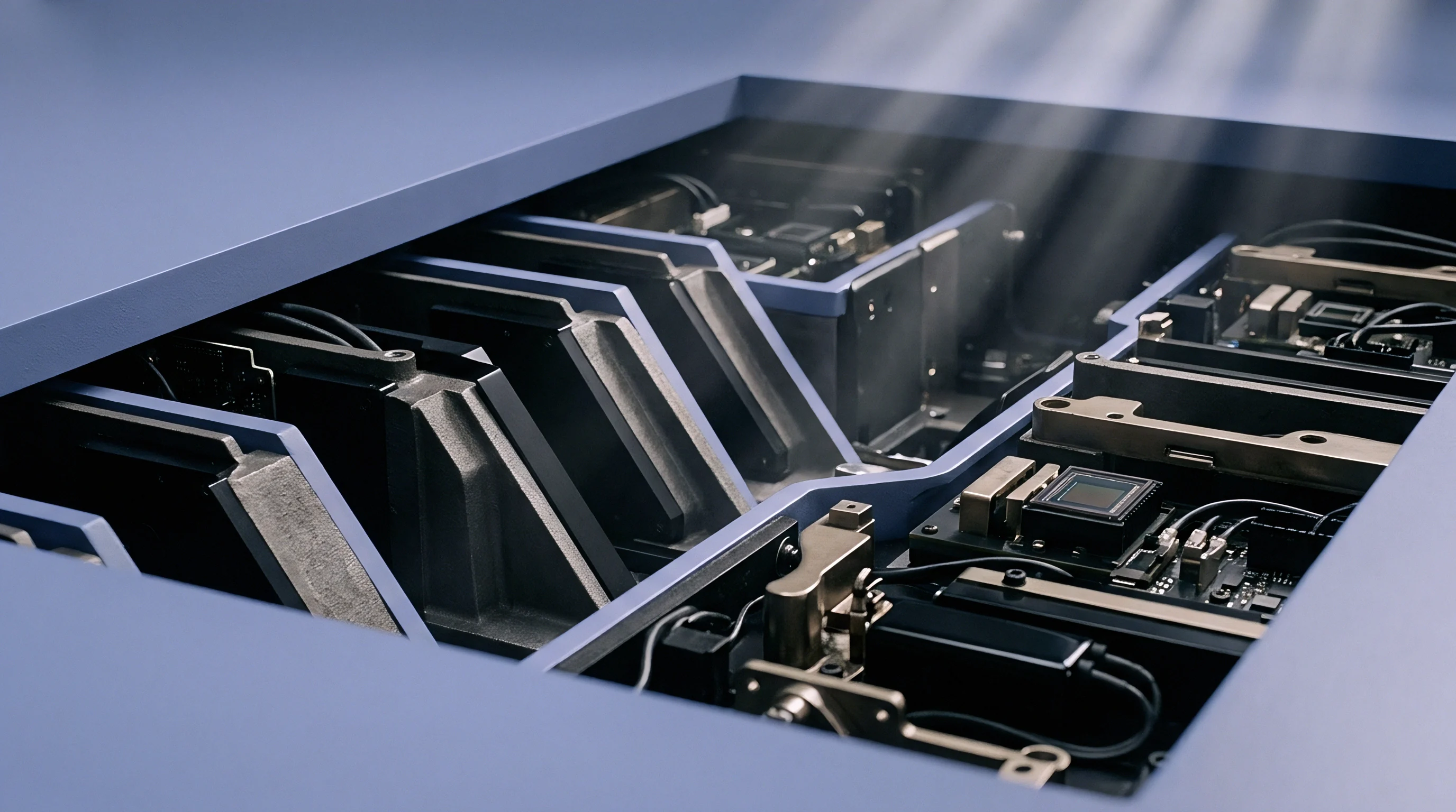
Packaging Form Tradeoffs and Mechanical Decoupling
Molded interposers isolate sensitive micro-electromechanical diaphragms from printed circuit board flexing. An LGA architecture incorporates a miniature printed circuit board within the sensor component itself. The solder joints connecting the package to the main system motherboard deform under thermal expansion, but this deformation spends its energy shearing the internal LGA substrate rather than bending the silicon die.
Interposers add height and unit cost.
Bare WLCSP designs forfeit this protective buffer layer. When board space restrictions force the selection of an ultra-thin WLCSP component, the hardware layout engineer must implement costly PCB slotting, routing isolation trenches around the sensor footprint to physically interrupt strain transmission paths. Routing mechanical relief trenches increases PCB fabrication panel costs by five to eight percent and consumes valuable routing area on inner board layers, eroding the footprint savings initially promised by the WLCSP package form.
| Package Format | Total Z-Height (Millimeters) | Board Area (Square Millimeters) | Thermal Hysteresis Error (Percent Full Scale) | 100k Unit Price (USD) | Integration Engineering Effort (Weeks) |
|---|---|---|---|---|---|
| Ultra-Thin WLCSP (50 um Die) | 0.35 | 1.44 | 1.85 | 0.28 | 6 to 8 |
| Overmolded LGA (100 um Die) | 0.85 | 4.00 | 0.45 | 0.48 | 2 to 3 |
| Cavity Metal-Lid LGA | 1.10 | 6.25 | 0.15 | 0.82 | 1 to 2 |
| Gel-Filled Stainless Probe | 4.50 | 28.00 | 0.02 | 3.45 | 0.5 |

Procurement Acceptance Gates and Thermal Proofing
Component purchase specifications state incoming baseline shift limits across twenty thermal excursion cycles. When purchasing ultra-thin sensor architectures, procurement teams often rely upon standard component-level datasheets that document parameters measured prior to surface-mount soldering. A vendor specification claiming zero-point accuracy of 0.1 percent applies only to loose components tested on custom zero-strain sockets.
Once reflowed onto production circuit boards, mechanical hysteresis frequently expands this error band tenfold.
Sourcing agreements must establish explicit board-level verification test vehicles. The incoming component quality contract should mandate that vendor qualification data include test measurements taken on four-layer standard FR4 test cards subjected to IPC-9701 thermal cycling conditions. Host firmware cannot predict board flex.
Commercial teams must factor the recurring cost of assembly-line thermal calibration stations against the initial purchase discount of bare wafer-level die variants.
Incorporating standard IPC-9701 paragraph 4.3 thermal cycle preconditioning into incoming purchase agreements reallocates the financial liability for board-level zero-point shift back to the component packaging supplier.