
Determining Break Even Volume Boundaries for Custom Sensor PCB Integration
Discrete sensor chip-down integration breaks even above fifteen thousand units where bill-of-materials savings overcome tooling and test fixture outlays.
Discrete sensor chip-down integration breaks even above fifteen thousand units where bill-of-materials savings overcome tooling and test fixture outlays.

Thermomechanical fatigue modeling for WLCSP solder arrays requires mapping viscoplastic Anand strain energy density to predict field thermal cycling failures.

Asymmetric thermal gradients across precision references induce microvolt offsets through Seebeck potentials and piezo-resistive stress imbalance.

Structure IC orders using exact full-reel increments matching historical baseline entitlements to bypass automated shortage allocation cuts.

Wafer level sensor package strain mitigation relies on compliant redistribution layers, optimized pad geometries, and firmware offset calibration to ensure operational stability.

Dynamic address assignment eliminates multiplexers in dense sensor arrays through cascade enable lines or software ARP, reducing PCB area while raising firmware bring-up requirements.

Selecting die packaging forms requires matching land pattern mechanical stress, bus wiring distance, and calibration stability against landed unit economics.

Board strain during reflow shifts MEMS digital offsets via CTE mismatch, requiring PCB keep-out zones, low-stress footprints, and 72-hour room-temp stabilization.
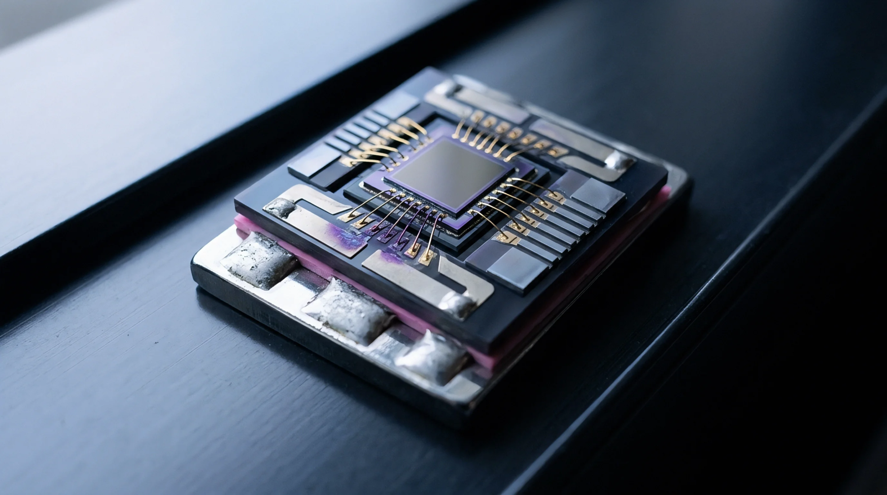
When component vendors end leaded packages, identical active silicon dies often survive in surface-mount forms that demand revised land patterns and thermal layouts.
Expertise is a utility, not a secret. sentiention™ publishes its working knowledge as open reference: intelligence layer covering the materials it sources, the markets it enters, and the reference that serves both.