Interfacial Shear Stress Mitigation inside Multi-Layer Sensor Cavity Geometries
Mitigate interfacial shear stress in cavity sensor packages by matching substrate thermal expansion and applying low-modulus decoupling layers.
Strain
Multi-layer sensor cavities bring together materials with starkly different thermal expansion coefficients. During board reflow or thermal cycling, this expansion mismatch creates severe shear stress across every bonded boundary. A silicon sensor die expands at roughly 2.6 parts per million per degree Celsius, while standard FR4 laminates expand laterally between 14 and 17 parts per million per degree Celsius.
Ceramic substrates like alumina narrow that gap with an expansion rate of 6.5 parts per million per degree Celsius. When these mismatched layers are joined by rigid adhesives, structural loads transfer directly into active transducer zones.
Thermal exposure during surface mount reflow alters joint bonds by accelerating expansion differences across materials. The resulting mechanical stress deforms piezoresistive bridges, shifts capacitive sensing gaps, and introduces uncalibrated offset drift. Peak lateral stress concentrates at the extreme corners of the die perimeter, where silicon is most vulnerable to fracturing.

Thermal Expansion Discrepancies across Substrate Interfaces
Substrate selection determines the magnitude of thermal mismatch across the cavity assembly. Relative to silicon’s low expansion rate of 2.6 parts per million per degree Celsius, organic PCB laminates introduce severe dimensional shifts. High-density interconnect designs using polyimide or advanced PTFE substrates exhibit lateral expansion values of 12 to 20 parts per million per degree Celsius.
By contrast, aluminum nitride substrates expand at 4.5 parts per million per degree Celsius, matching silicon far more closely than alumina does. How much of this differential reaches the die depends on the thickness and shear modulus of the attach layer.
| Substrate Layer Material | Expansion Coefficient (ppm/°C) | Shear Modulus (GPa) | Peak Interfacial Stress (MPa) |
|---|---|---|---|
| Silicon Transducer Die | 2.6 | 68.0 | 0.0 |
| Standard FR4 Laminate | 16.0 | 18.0 | 112.5 |
| Polyimide Flex Substrate | 15.0 | 4.2 | 64.0 |
| Alumina Ceramic (96% Al2O3) | 6.5 | 300.0 | 48.2 |
| Aluminum Nitride (AlN) | 4.5 | 330.0 | 22.1 |

Shear Gradient Distribution in Cavity Ledges
Mechanical forces concentrate along the physical boundary where the silicon perimeter meets the cavity ledge. Edge effects create multi-axial stress fields with both normal peel and in-plane shear components, the latter acting parallel to the bond plane to drive lateral movement across the adhesive. Stress concentration calculations show that right-angled cavity corners multiply localized shear force by factors between 2.4 and 3.1 compared to central die regions.
Using ceramic substrates helps lower the overall expansion delta, while corner chamfers and rounded ledge step geometries redistribute force vectors over broader surface areas.
Peak interfacial stress along a 4 mm silicon die edge reaches 82 MPa during thermal cycling from -40 °C to 125 °C when bonded directly to alumina.
Variations in adhesive thickness directly alter physical tilt, as non-uniform die attach fillets create asymmetric stress profiles across sensitive piezoresistive diaphragms. When one edge of a sensor die experiences greater restraint than the opposite side, thermal changes induce bending moments across the diaphragm plane that mimic pressure inputs, generating false readings at the host system interface. Maintaining strict bond line thickness control mitigates these asymmetric force distributions.
Ignoring these coefficient mismatches leads to die cracking during reflow, shifting zero-point outputs and ruining factory calibration data.

Compliance
Low-modulus decoupling materials absorb mechanical displacement before strain reaches the sensing element. Elastomeric die attach compounds, soft fluorosilicone gels, and thixotropic adhesives serve as mechanical dampers within the package cavity. Because polymers exhibit viscoelastic behavior ~ their modulus dropping sharply above the glass transition temperature ~ choosing decoupling materials with glass transition points below the minimum operating temperature preserves compliance across the entire environmental range.
Gel viscosity dictates how cleanly material fills cavity trenches. Soft cavity fills isolate transducers while shielding wire bonds from ambient moisture. The overall compliance of an elastomer layer scales inversely with its thickness and shear modulus: thinner bond lines transfer heavier shear loads into the silicon die, whereas thicker layers introduce tilt variability during surface-mount placement.

Elastomeric Buffer and Underfill Formulations
Soft die attach adhesives use silicone or modified epoxy chemistries to keep Young’s modulus values under 50 MPa, in contrast to standard epoxy adhesives whose rigid moduli exceed 3000 MPa and transmit expansion forces directly to the die. Silicone formulations maintain this low modulus down to -55 °C, preserving structural compliance during deep thermal cycling. Meanwhile, fluorosilicone gels fill cavity voids around sensitive MEMS diaphragms without imposing measurable restraint on sensor movement, though moisture absorption can still cause organic polymers to swell.
- Die Corner Delamination ~ Thermal cycling separates the adhesive bond along peripheral edges, leading to localized stress concentrations and output hysteresis.
- Piezoresistive Offset Drift ~ Mechanical force transmitted through die attach layers deforms bridge resistors, shifting zero-pressure baseline voltages.
- Wire Bond Heel Cracking ~ Shear movement between the substrate and die surface causes fatigue fractures in aluminum interconnect wires at the bond pad interface.
- Cavity Seal Rupture ~ Differential thermal expansion across package lids breaches hermetic seals, exposing sensitive MEMS structures to atmospheric moisture.
Thicker adhesive bond lines lower force transfer across material layers but increase physical tilt errors across the active sensor plane.
Decoupling gels require precise dispensation to prevent migration onto sensitive optical surfaces or piezoresistive diaphragms. Overdispensing increases the effective mass of resonant sensor elements and shifts their frequency response, while underdispensing leaves die edges vulnerable to mechanical shock and unmitigated substrate shear. Automated dispensing keeps volumetric accuracy within plus or minus two percent.
Post-reflow offset shifts stem from adhesive modulus creep as well as board assembly thermal profiles.


Geometry
Targeted structural changes inside the package cavity alter force transmission paths. Machining stress-relief trenches into substrate ledges interrupts direct mechanical coupling between rigid package sidewalls and die edges. Recessed mounting pedestals elevate the die landing pad so excess adhesive drains freely into surrounding channels, preventing fillet creep up sidewalls and confining the bond strictly to the bottom silicon surface.
Substrate stack-up design directly governs overall package stiffness. Asymmetric layer counts lead to thermal warpage during reflow cooling, whereas balanced copper layouts in organic substrates eliminate bowing. Maintaining a flat landing zone in this way prevents localized shear spikes along die perimeters.
Why Do Polymer Cavity Sealants Shift Baseline Strain?
Curing shrinkage in organic compounds generates residual tensile stress across internal surfaces. As polymer chains cross-link during thermal curing, volumetric contraction creates permanent internal stress that pulls die edges inward toward the center of the adhesive pad. Selecting low-shrinkage formulations with volumetric contraction below 0.5 percent minimizes these post-cure baseline shifts.
| Feature Architecture Type | Width Tolerance (µm) | Depth Tolerance (µm) | Peak Shear Reduction (%) |
|---|---|---|---|
| Flat Surface Cavity (Baseline) | ±10.0 | N/A | 0.0 |
| Peripheral Relief Moat | ±5.0 | ±2.5 | 38.5 |
| Elevated Center Pedestal | ±8.0 | ±3.0 | 52.0 |
| Dual Stepped Ledge Trench | ±4.0 | ±2.0 | 64.5 |
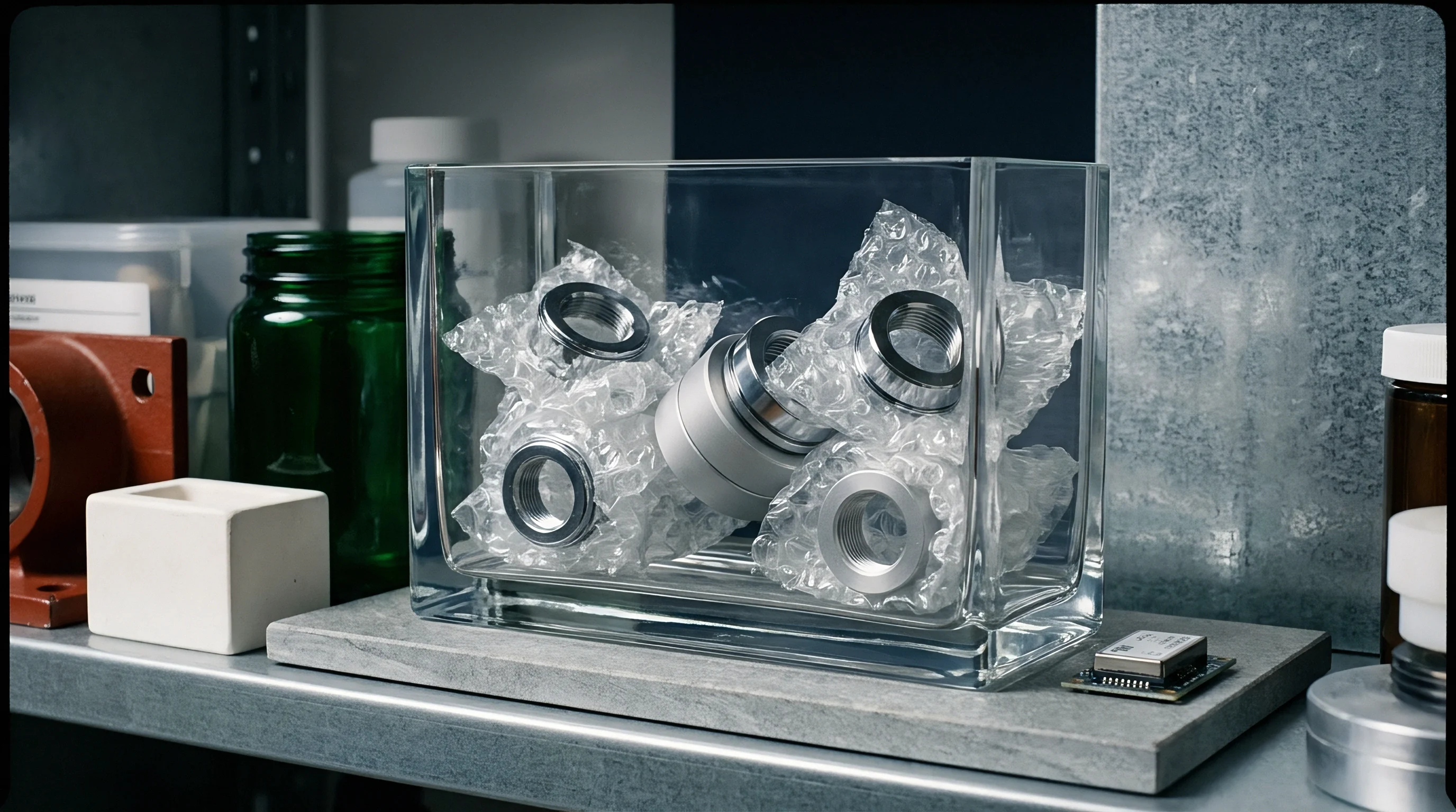
Stress Isolation Moats and Perimeter Fillets
Etched channels in ceramic or silicon bases create physical breaks that divert thermal stresses away from active sensor zones. Isolation moats surrounding the die pad decouple central mounting locations from package wall deformation. In silicon substrates, deep reactive ion etching yields narrow moats with aspect ratios exceeding ten to one, blocking lateral force propagation while preserving structural integrity.
- Etch perimeter isolation channels 150 micrometers wide and 50 micrometers deep into the substrate ledge using plasma dry processing.
- Dispense high-purity fluorosilicone gel into the central recess with an automated needle system, submerging die surfaces while leaving bond pads exposed.
- Perform thermal curing at 150 °C for 120 minutes in a nitrogen purge oven to achieve stable cross-linking without introducing voids.
JEDEC JESD22-A104 test conditions mandate 1000 thermal cycles between -40 °C and 125 °C to qualify package physical integrity.
Fillet geometry controls perimeter stress concentrations. Adhesive fillets that rise beyond half the die height create top-edge mechanical constraints, inducing bending moments across active sensing zones. Keeping fillet height below 30 percent of total die thickness confines shear stress to lower silicon regions, well clear of top-surface sensing structures.
Production lines rely on automated optical inspection to verify fillet height compliance.
Specifying IPC-7093 Class 3 voiding limits below five percent under bottom-terminated dies restricts localized stress points and prevents premature bond failure.
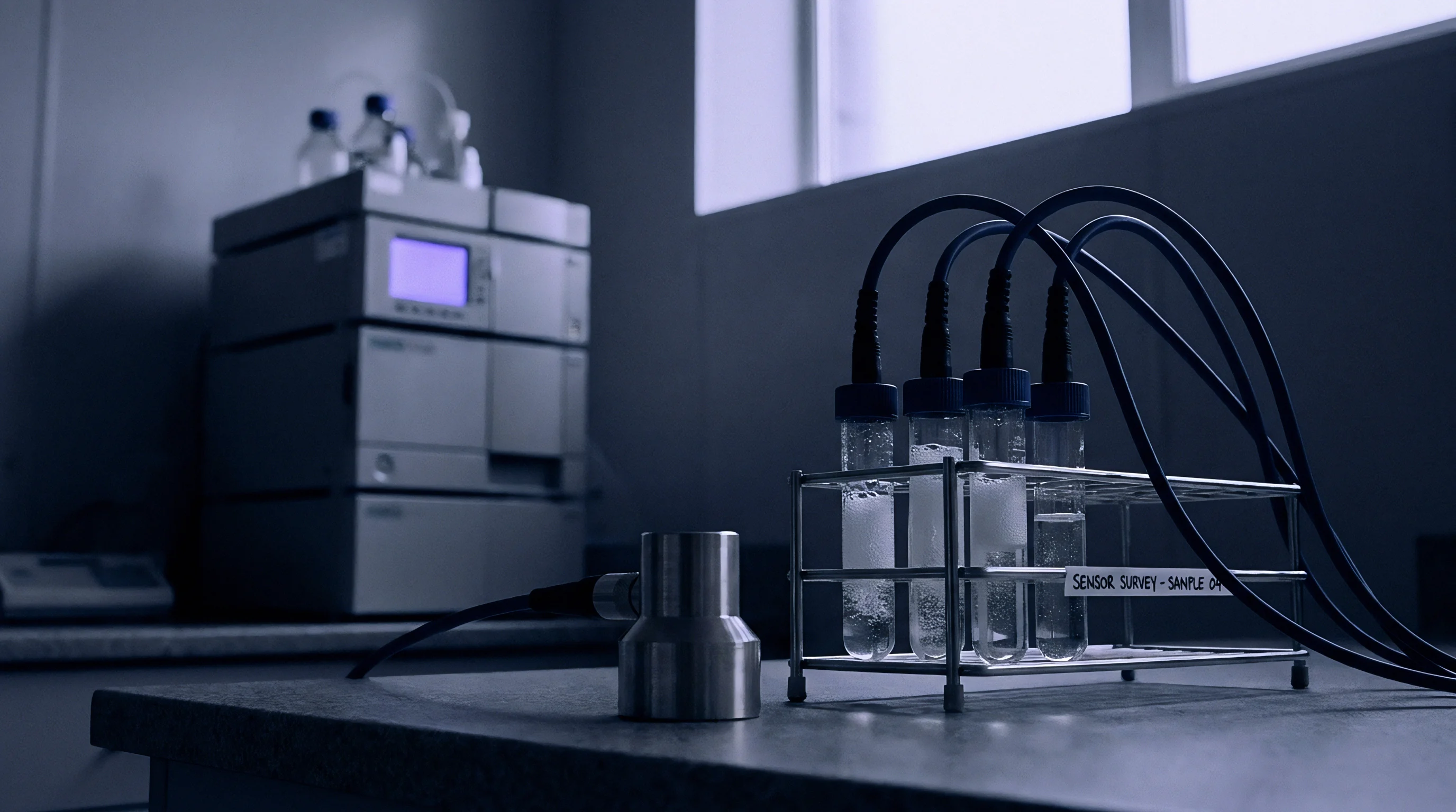

Compensation
Host microcontrollers rely on digital correction algorithms to neutralize thermal shifts. Because residual mechanical stress alters zero-point baselines and span sensitivity slopes across temperature ranges, modern digital sensor interfaces embed temperature sensors directly alongside transducer elements. These temperature readings feed real-time polynomial algorithms that calculate stress-induced signal shifts and continuously update output registers.
Because register writes consume processing cycles and bus clock speeds govern throughput, host processors reading raw pressure and temperature values over digital buses must efficiently apply correction parameters stored during factory calibration. High-speed SPI interfaces complete recalibration loops faster than slower I2C buses, cutting overall system input latency.

Register Map Structure for Stress Offsets
Internal memory arrays store the polynomial correction factors calculated during factory calibration. By mapping device behavior across the operating temperature range, multi-point calibration establishes offset slope and curvature coefficients that are saved to EEPROM. At boot, on-chip signal processing ASICs retrieve these coefficients and run matrix calculations on raw transducer streams before updating output registers.
| Interface Bus Protocol | Clock Ceiling (kHz) | Firmware Overhead (Weeks) | Data Retrieval Latency (µs) |
|---|---|---|---|
| Standard I2C Bus | 400 | 2.5 | 180.0 |
| Fast Mode Plus I2C | 1000 | 2.5 | 72.0 |
| Four-Wire SPI Bus | 10000 | 4.0 | 12.5 |
| Single-Edge Analog Output | N/A | 0.5 | 2.0 |

Digital Filtering of Thermally Induced Output Shifts
Firmware routines apply low-pass infinite impulse response filters to smooth rapid signal swings during thermal ramps. Temperature transients induce temporary mechanical stress gradients across sensor cavities, producing brief output spikes until internal equilibrium is reached. Digital filtering dampens these spikes, keeping host controller responses within nominal error bands during rapid thermal transitions.
- Board Space Constraints ~ Compact surface-mount layouts favor integrated signal-conditioning ASICs over discrete analog compensation components.
- Firmware Lead Time ~ Standardized I2C register maps enable reusable driver modules, shortening bring-up across new sensor designs.
- Thermal Cycle Demands ~ Automotive applications specify real-time polynomial drift calculation to offset material relaxation over extended lifespans.
- Yield Loss Allocation ~ Factory calibration time directly drives up unit manufacturing costs, making multi-point thermal testing a primary cost contributor.
Residual strain inside a package cavity behaves as an uncalibrated strain gauge mounted directly to the active transducer element.
Updating compensation registers while active readings are being pulled over the digital bus can corrupt data if bus transactions overlap internal calculation cycles. Implementing dual-buffer register schemes prevents the host from reading partially updated parameters during background recalculations.
Dynamic polynomial calibration in host firmware may not fully eliminate long-term viscoelastic relaxation drift in filled cavities.
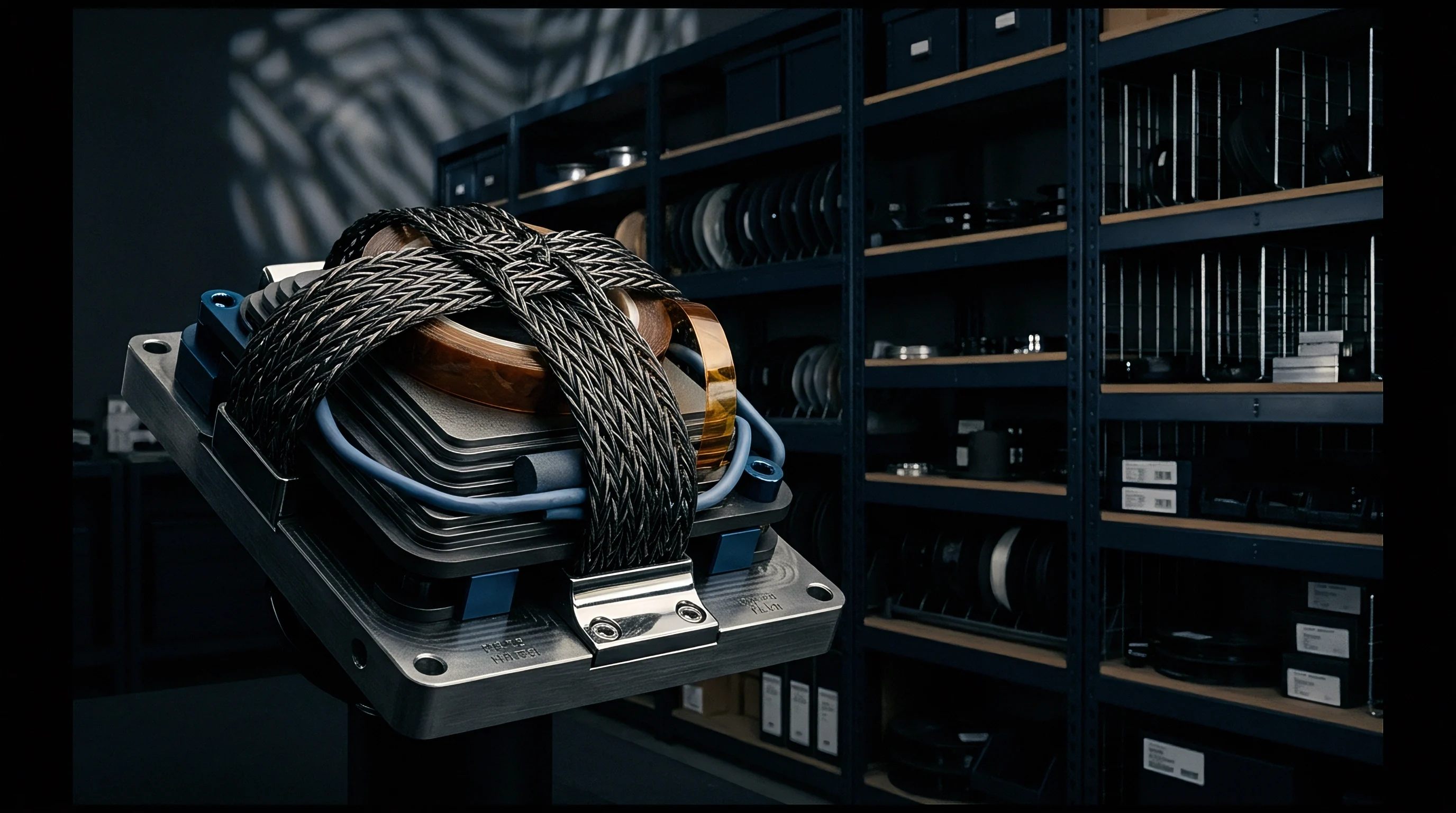
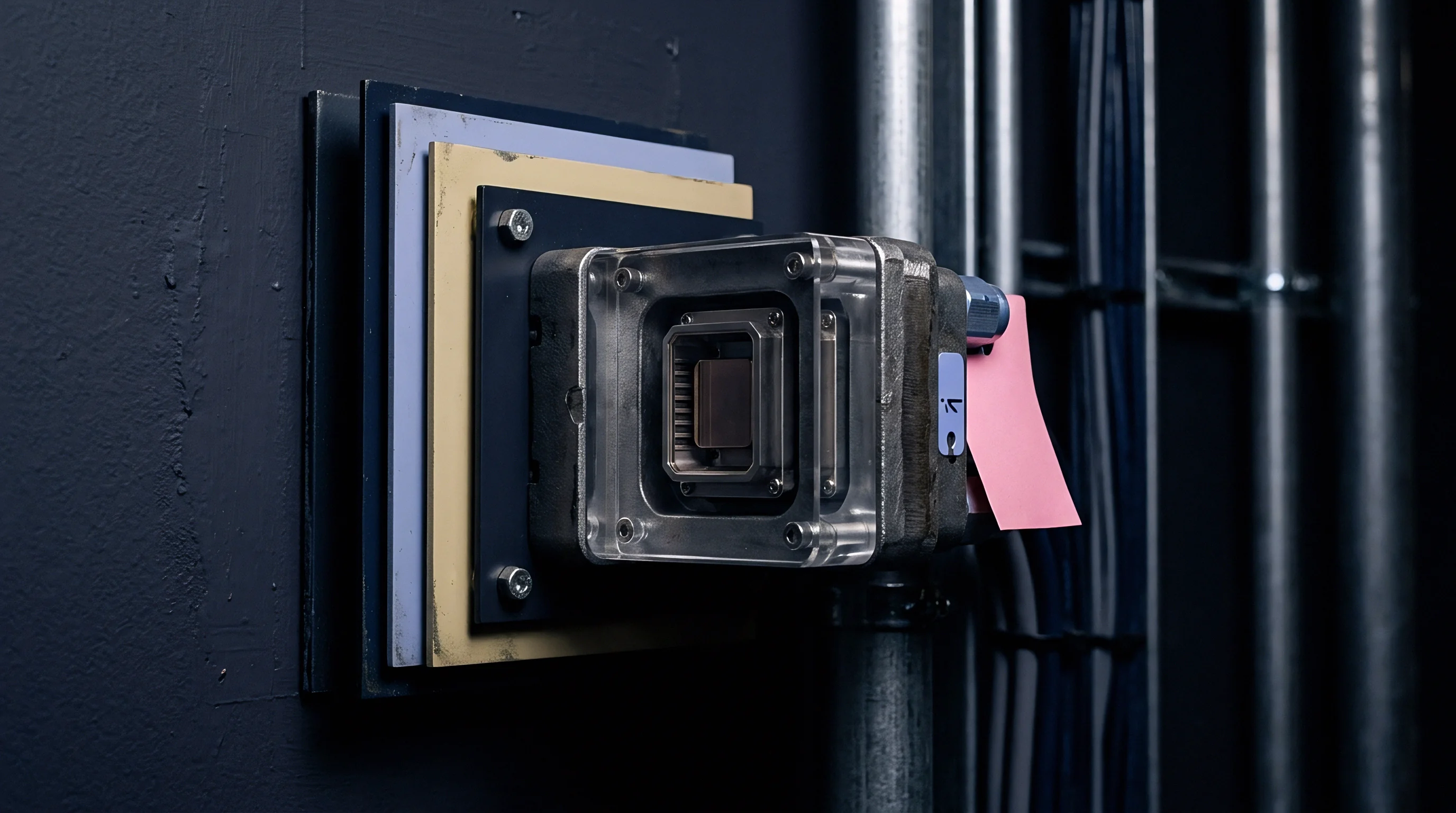
Valuation
Component selection balances piece-part prices against integration labor and warranty exposure. Sourcing raw silicon dies in basic surface-mount packages keeps upfront component costs low but demands substantial engineering effort to implement board-level stress isolation. Conversely, integrated cavity modules pre-filled with elastomeric gels carry higher unit prices while shifting thermal strain mitigation to the package vendor.
While tooling costs scale with volume and yield losses drive overall expense, sourcing bare die requires dedicated cleanroom infrastructure. In high-reliability applications, lower warranty return rates over extended operating lifespans often justify the higher initial cost of ceramic cavity packages.

Package Form Cost Spreads and Minimum Quantities
Raw silicon dies in wafer form carry the lowest initial component cost, though wafer-level purchasing requires dedicated cleanroom die-attach tools, automated gel dispensing lines, and multi-point temperature calibration chambers. Surface-mount LGA packages add substrate and lid expenses that raise baseline unit costs by 180 to 240 percent over bare dies. Fully sealed, gel-filled standalone modules represent the highest piece-part expense ~ often ten to fifteen times the cost of raw dies ~ but eliminate package-level assembly on the buyer’s line.
Minimum order quantities vary widely by package type. Bare wafers demand full-wafer commitments that often exceed 5000 units per fabrication run. Standard QFN and LGA surface-mount packages ship on tape-and-reel with typical minimum orders of 1000 to 3000 units.
Custom gel-filled modules carry higher order thresholds to offset factory setup charges, forcing buyers to amortize non-recurring engineering fees across production runs.

Make against Buy Breakeven Arithmetic
Building custom cavities requires upfront tooling investments exceeding fifty thousand dollars, alongside 16 to 24 engineering weeks to stabilize automated gel dispensing and multi-point calibration processes. Assuming an integrated gel-filled module costs $14.50 delivered versus $4.20 in bill-of-materials costs for an in-house surface-mount LGA design, amortizing $60,000 in tooling and $80,000 in engineering labor places the make-or-buy break-even point near 13,600 units.
At volumes below 13,600 units, buying pre-packaged, pre-calibrated standalone modules avoids upfront capital expenditure and saves engineering time. Above 50,000 units, the unit cost savings of developing a custom multi-layer cavity design justify the initial outlay while keeping packaging IP in-house.
Purchasing pre-calibrated standalone sensor modules shifts warranty liability and yield management directly to the component vendor.