Mechanical Stress
A physical deformation occurs when a printed circuit board experiences bending forces during assembly or operation. This board flexure can crack ceramic capacitors and solder joints. Structural strain typically arises from screw attachment or manual handling of the panel.
Design guidelines restrict the allowable deflection to prevent electrical failure.
Strain Measurement
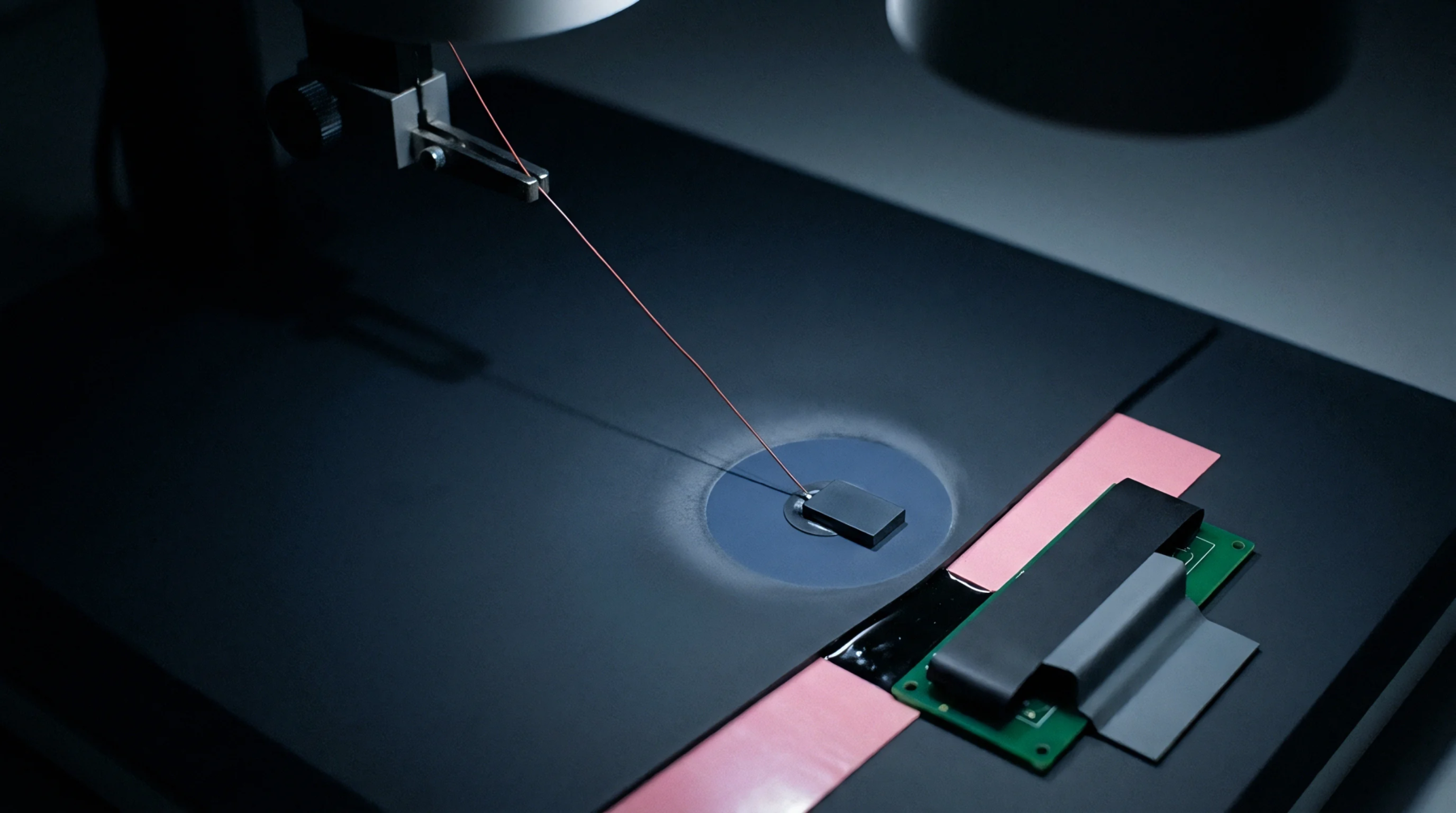
Engineers use miniature strain gauges bonded to the board surface to quantify the deformation during mechanical operations. The measured microstrain represents the fractional change in length of the board material under load. Industry standards establish maximum allowable strain limits based on the thickness of the board and the types of components attached to it.
Defection Evaluation
Testing involves applying a localized force to a supported board to measure the resulting displacement and the strain at critical component locations. These trials determine the vulnerability of specific layouts to bending damage. Inadequate support during routing or transport causes excessive deflection.
Circuit designers must position sensitive components away from high strain areas such as mounting holes and edge connectors to minimize risk.
Failure Mitigation
Placing stiffening rails or optimizing the routing of copper layers increases the structural rigidity of the assembly. Flexible solder alloys can also accommodate higher levels of deformation without cracking. Ensuring adequate support fixtures during automated testing reduces mechanical strain.