Low Temperature Solder Dynamic Strain Rate Mechanics
Bismuth segregation at copper intermetallic boundaries induces brittle cleavage under rapid drop shock, demanding microalloyed dopants to preserve high-velocity toughness.

Impact
Mechanical shock exposes an immediate physical weakness in low-temperature electronics assembly. When a portable device slips or hits a rigid surface, the printed circuit board decelerates violently, sending transient flexural waves through copper traces, dielectric cores, and solder ball arrays. Standard tin-lead and tin-silver-copper joints absorb these sudden displacements through extensive dislocation movement, blunting crack tips with rapid localized plastic deformation.
Eutectic tin-bismuth solders, chosen to drop peak reflow thermal profiles from 245°C down to 170°C, react quite differently under sudden kinetic impact.
Peak board acceleration can reach fifteen hundred gravities. Board strain rates during drop events fall between 1.0 and 100 reciprocal seconds ~ orders of magnitude above the quasi-static creep seen in standard thermal cycling. Solder joints take severe tensile shock.
Under static shear or low-velocity pull tests, eutectic 58Bi-42Sn solder shows measurable ductility, yielding gradually across its bulk lamellar phases. Once displacement speed rises, the deformation mode shifts abruptly from ductile bulk elongation to catastrophic interfacial separation.
Tin-bismuth solder balls subjected to strain rates above ten reciprocal seconds lose eighty percent of their plastic deformation energy compared to static tensile loading.
Solder balls at package corners take the highest normal peeling stresses during flexural vibration. As the printed circuit board flexes downward, the outermost joints carry concentrated tensile loads while internal joints remain under compressive or low shear stress. When standard packaging lines replace conventional SAC305 balls with eutectic tin-bismuth paste or paste-ball combinations, high deformation speeds change where joints fail.
Rather than absorbing transient bending through bulk solder yielding or trace necking, low-temperature joints split along the boundary between the bulk solder and the underlying intermetallic compound layer.
Strain Rate Velocity Thresholds in Bismuth Alloys
The mechanical response of tin-bismuth alloys depends directly on strain velocity. At low speeds, grain boundary sliding lets individual bismuth-rich phases rotate and deform alongside the tin matrix, dispersing mechanical energy through the bulk ball. Pushing up the strain rate suppresses this mechanism because dislocation velocity inside the rhombohedral bismuth lattice cannot keep pace with the applied displacement.
- Quasi-static creep loading operates below 0.001 reciprocal seconds, allowing full dislocation climb, grain boundary sliding, and stable plastic deformation across the two-phase microstructure without premature voiding.
- Intermediate board flexure occurs between 0.01 and 1.0 reciprocal seconds during automated depaneling or test socket actuation, forcing the tin matrix into dislocation glide while rigid bismuth particles act as internal stress concentrators.
- Transient shock impact spans rates from 1.0 to 50 reciprocal seconds during product drops, driving localized shear bands that cause immediate brittle cleavage along crystallographic planes within the bismuth phase.
- Ballistic mechanical shock exceeds 100 reciprocal seconds under severe shock environments, triggering instant interfacial crack propagation along intermetallic boundaries with almost no plastic deformation in the bulk solder.
Stiffer substrates amplify interfacial shear stresses. When high-modulus package substrates connect to thin consumer circuit boards, the stiffness mismatch drives almost all bending energy straight into the solder joint perimeter. Pad geometry dictates how those peeling stresses distribute during board resonance.
Non-solder mask defined land patterns expose the copper pad sidewalls, spreading tensile stress over a wider radius and lowering stress intensity under rapid bending.

Board Deflection Induced Ball Grid Cleavage
Cleavage cracks initiate within the first two milliseconds of substrate acceleration. Strain gauge rosettes placed next to corner ball positions record transient board flexure exceeding fifteen hundred microstrain during standard drop hammer tests. If the solder metallurgy lacks enough dynamic ductility, cracks form at the outer notch where solder mask meets the joint boundary, running horizontally through the intermetallic interface before the board even completes its first downward flex.
Misjudging the shock strain limit on outer solder balls leads to immediate pad lifting during early qualification drops, scrapping prototype board runs and delaying release by months.


Bismuth
How elements distribute inside solidifying solder joints establishes their underlying rate sensitivity. Cooling down from reflow temperatures, tin and bismuth form a eutectic microstructure of alternating lamellar plates ~ tetragonal beta-tin and rhombohedral bismuth. Pure bismuth has low solid solubility in tin at room temperature, staying below 1.5 weight percent under equilibrium cooling.
But factory assembly lines cool far from thermodynamic equilibrium, trapping excess bismuth directly inside the tin lattice.
Fast cooling refines the lamellar colony structure. Pulling heat out quickly during reflow limits the time bismuth atoms have to segregate into distinct lamellae, producing fine microstructures with higher room-temperature shear strength. Ambient storage, however, destabilizes this metastable solution.
Over weeks on the shelf, supersaturated bismuth precipitates out of the tin lattice into micro-particles that pin dislocation movement and harden the joint, while remaining bismuth migrates toward the copper-tin intermetallic interface.
Rapid cooling suppresses coarse bismuth lamellae but leaves substantial residual stresses inside the tin matrix.
Lamellar bismuth plates shear along crystallographic planes. Bismuth’s rhombohedral crystal structure has few available slip systems compared to body-centered tetragonal tin, leaving the bismuth phase brittle under fast tensile loading. When sudden mechanical strain drives rapid movement through the alloy matrix, dislocations pile up at phase boundaries between tin and bismuth.
Because bismuth crystals cannot deform plastically at high speeds, stress builds at these boundaries until micro-cracks open parallel to the shear vector.
| Alloy Composition | Yield Strength at Low Strain Rate (MPa) | Tensile Strength at High Strain Rate (MPa) | Strain Rate Sensitivity Exponent | Dynamic Elongation at Break (%) |
|---|---|---|---|---|
| Sn42Bi58 Eutectic | 68 ± 4 | 112 ± 8 | 0.085 ± 0.006 | 4.2 ± 0.8 |
| Sn42Bi57Ag1 | 74 ± 5 | 124 ± 9 | 0.078 ± 0.005 | 6.5 ± 1.1 |
| Sn40Bi56In4 | 58 ± 4 | 96 ± 7 | 0.095 ± 0.007 | 11.4 ± 1.5 |
| SAC305 Reference | 32 ± 3 | 78 ± 6 | 0.042 ± 0.003 | 28.5 ± 2.6 |
Solid Solution Hardening and Interfacial Segregation
Precipitation of dissolved bismuth changes interconnect fracture toughness. The strain rate sensitivity exponent, m, measures how yield stress rises with deformation speed. Tin-bismuth alloys show higher m values than standard SAC305.
A higher exponent means the material strengthens sharply as loading velocity increases, pushing yield stress past the theoretical cleavage strength of phase boundaries before plastic deformation can dissipate the energy.
- Metastable trapping occurs during reflow solidification, retaining up to four weight percent bismuth in solid solution inside the dendritic tin matrix.
- Ambient precipitation progresses during room-temperature storage, forming nanoscale bismuth clusters that block dislocation movement and increase bulk hardness.
- Interfacial migration pushes mobile bismuth atoms toward the copper stannide reaction front, leaving a continuous, sub-micron film of pure bismuth behind the intermetallic scallops.

Can Controlled Cooling Rates Suppress Bi Segregation?
Adjusting the cooling slope in reflow ovens changes the scale of phase separation. Ramp rates between 3°C and 5°C per second keep lamellar spacing below two micrometers, spreading interfacial stress over more surface area. Slower cooling around 1°C per second creates coarse bismuth colonies larger than ten micrometers.
Under sudden shock, these coarse colonies yield long, uninterrupted cleavage facets that split solder joints with almost no energy absorption.
Fine lamellar dispersion alone does not guarantee drop reliability; aged field assemblies continue showing interfacial cleavage under moderate physical impacts.

Fracture
Cracks in low-temperature solder joints follow distinct mechanical paths set by strain velocity. At crosshead speeds below one millimeter per minute, fractures wander through the bulk solder, working through ductile tin phases and showing high plastic elongation. Once crosshead speeds exceed five hundred millimeters per second during high-speed ball pull or shear testing, failure shifts directly to the package or board metallization boundary.
Brittle cleavage replaces ductile void coalescence. The intermetallic layer between eutectic tin-bismuth solder and copper pads consists mostly of eta-phase Cu6Sn5 scallops. Extended reflow or repeated thermal cycles build a secondary layer of epsilon-phase Cu3Sn between the Cu6Sn5 and the underlying copper pad.
Neither intermetallic compound absorbs shear deformation; both have high elastic moduli and low fracture toughness, acting as rigid ceramic barriers under transient stress waves.
Testing under JEDEC JESD22-B111 condition B penalizes stiff intermetallic boundaries by delivering a half-sine shock of fifteen hundred gravities in zero point five milliseconds.
Interfacial cracks advance through the copper stannide layers. When high-velocity shock hits the joint, stress waves create heavy shear where scalloped Cu6Sn5 intermetallics meet bulk solder. In tin-bismuth joints, bismuth rejection weakens this boundary.
Because copper has virtually zero solubility in bismuth, Cu6Sn5 growth pushes nearby bismuth atoms outward, concentrating pure bismuth in intermetallic valleys. That rejected bismuth layer functions as a built-in pre-crack under shock loading.
| Pad Surface Finish | Intermetallic Species | IMC Layer Thickness (µm) | Brittle Cleavage Mode Share (%) | Drop Cycles to Failure (JESD22-B111) |
|---|---|---|---|---|
| Organic Solderability Preservative (OSP) | Cu6Sn5 | 1.8 ± 0.3 | 62 ± 5 | 140 ± 18 |
| Electroless Nickel Immersion Gold (ENIG) | (Ni,Cu)3Sn4 | 2.4 ± 0.4 | 84 ± 6 | 75 ± 12 |
| Electroless Nickel Electroless Palladium Immersion Gold (ENEPIG) | (Pd,Ni)Sn4 / (Ni,Cu)3Sn4 | 1.9 ± 0.2 | 48 ± 4 | 185 ± 22 |
| Immersion Silver (ImAg) | Cu6Sn5 | 1.6 ± 0.2 | 55 ± 5 | 160 ± 19 |
| Failure modes determined by scanning electron microscopy per JEDEC JESD22-B117A at 1000 mm/s shear speed on 400 µm pitch ball arrays. | ||||
Intermetallic Boundary Cleavage under Rapid Board Bending
Surface finishes shape the chemistry and structure of the brittle boundary. On copper pads with organic solderability preservatives, the intermetallic forms rough Cu6Sn5 scallops that offer mechanical interlocking under shear. On electroless nickel immersion gold finishes, the reaction product forms a flat layer of Ni3Sn4 or (Ni,Cu)3Sn4.
This flat morphology provides minimal interlocking, allowing cracks to travel straight across during board deflection.
Gold embrittlement compounds bismuth segregation defects. Gold dissolved from ENIG surface finishes forms AuSn4 intermetallics floating in bulk solder. During sudden board impact, these needle-like AuSn4 structures act as stress concentrators, starting tertiary cracks that link with the primary cleavage path moving along the nickel stannide interface.
Will Nickel Additions Alter Interfacial Fracture Energy?
Doping solder paste with trace nickel slows intermetallic dissolution and smooths the reaction front. Small amounts of nickel stabilize the (Cu,Ni)6Sn5 phase, preventing phase transformations during thermal cycling. This stabilization cuts micro-void formation along the intermetallic interface, raising the energy needed to propagate a cleavage crack under rapid shock loading.
Whether atomic dopants can completely stop bismuth migration to the copper stannide boundary during long-term thermal aging remains an open question in interconnect metallurgy.


Dopants
Alloying modifications offer a practical strategy for improving the shock resistance of low-temperature interconnects. Binary Sn42Bi58 prints well and reflows at low temperatures, but its dynamic fracture energy falls short of consumer drop standards. Introducing small amounts of silver, antimony, nickel, indium, or rare earth elements alters dislocation behavior and grain structure within the binary alloy.
Antimony dissolves into the tin lattice, substituting directly for tin atoms to provide solid solution strengthening while increasing bismuth solubility. That higher solubility prevents room-temperature precipitation of brittle bismuth colonies, preserving dynamic compliance in tin-rich areas. Silver additions form dispersed Ag3Sn intermetallic spheres that pin grain boundaries without creating planar cleavage interfaces.
Adding trace nickel preserves joint toughness during rapid shock loading by migrating directly to the intermetallic interface.
Resin formulations protect the outer joint boundary. Beyond metallic dopants, epoxy resin systems can be blended into low-temperature solder pastes. During reflow, flux cleans surface oxides before the epoxy polymerizes and flows outward to form a protective collar around the solder fillet.
This cured collar redistributes mechanical stress away from the fragile intermetallic boundary during board bending, noticeably increasing drop survival.
| Alloy and Modifier Designation | Melting Range Solidus/Liquidus (°C) | Raw Solder Paste Cost Relative to SAC305 | Drop Shock Survival Ratio (Cycles to Failure Normalized to SAC305) | Primary Toughening Mechanism |
|---|---|---|---|---|
| Sn42Bi58 Binary Baseline | 138 / 138 | 0.72 | 0.22 | None (Unmodified Eutectic) |
| Sn42Bi57Ag1 Microalloyed | 137 / 139 | 0.88 | 0.48 | Ag3Sn Dispersion Hardening |
| Sn42Bi56.5Ag1Ni0.5 | 138 / 141 | 0.94 | 0.65 | IMC Refinement and Planar Stabilization |
| Sn40Bi55In4Sb1 Ductile Matrix | 132 / 138 | 1.45 | 0.82 | Matrix Softening via Indium Solid Solution |
| Sn42Bi58 + 12% Epoxy Resin Flux | 138 / 138 | 1.28 | 0.95 | Polymer Corner Fillet Stress Redistribution |
Microalloying Elements and Microstructure Refinement
Grain refinement directly improves dynamic fracture resistance. Trace titanium or cobalt added below zero point one weight percent acts as heterogeneous nucleation sites during solidification. The resulting microstructure forces propagating cracks to repeatedly change direction, consuming far more energy during high-velocity impacts.
- Indium alloying additions lower matrix shear modulus, increasing dynamic ductility by promoting deformation twinning under high shock loads.
- Silver microalloying agents generate sub-micron Ag3Sn particulates that intercept dislocation cascades, keeping slip bands from concentrating stress along weak phase boundaries.
- Nickel interfacial modifiers migrate quickly to copper reaction interfaces, forming thin barrier layers that block bismuth accumulation behind intermetallic scallops.
- Polymer resin inclusions bleed outward during liquidus reflow, curing into a structural fillet that cuts peel stress on package corners.
Ductile Matrix Modification via Antimony and Silver
Balancing dopant concentration requires tight process control. Adding too much silver or nickel forms coarse primary intermetallic needles in the bulk solder before general solidification begins. These large needles act as internal stress concentrators, worsening shock performance instead of improving it.
Keeping silver around one percent and nickel below zero point zero five percent achieves grain refinement without causing primary phase embrittlement.
Solder paste costs jump thirty percent. Moving from binary Sn42Bi58 to multi-component doped alloys or resin-reinforced pastes shifts the economic balance. While solder costs rise, the premium is offset by eliminating board warpage, reducing oven energy consumption, and lowering field failures from mechanical drops.
Alloys that suppress interfacial bismuth precipitation hold up reliably under severe drops regardless of component footprint orientation.


Screening
Verifying dynamic fracture resistance requires test methods that mirror the strain rates of actual field drops. Standard quasi-static ball shear tests, run at speeds between zero point one and one millimeter per second, fail to catch brittle cleavage. At low speeds, plastic flow dissipates applied stress, showing acceptable shear strength on joints that would cleave catastrophically in a drop.
High-speed ball shear tests isolate brittle failure. Running shear assessments at velocities between one thousand and three thousand millimeters per second pushes solder joints into high strain rate regimes. Specialized test heads strike individual balls while recording load-displacement curves with microsecond time resolution.
Integrating the force-displacement curve up to rupture gives total fracture energy, which serves as the key qualification metric. Joints failing by brittle interfacial cleavage show abrupt load drops and almost no post-peak energy absorption.
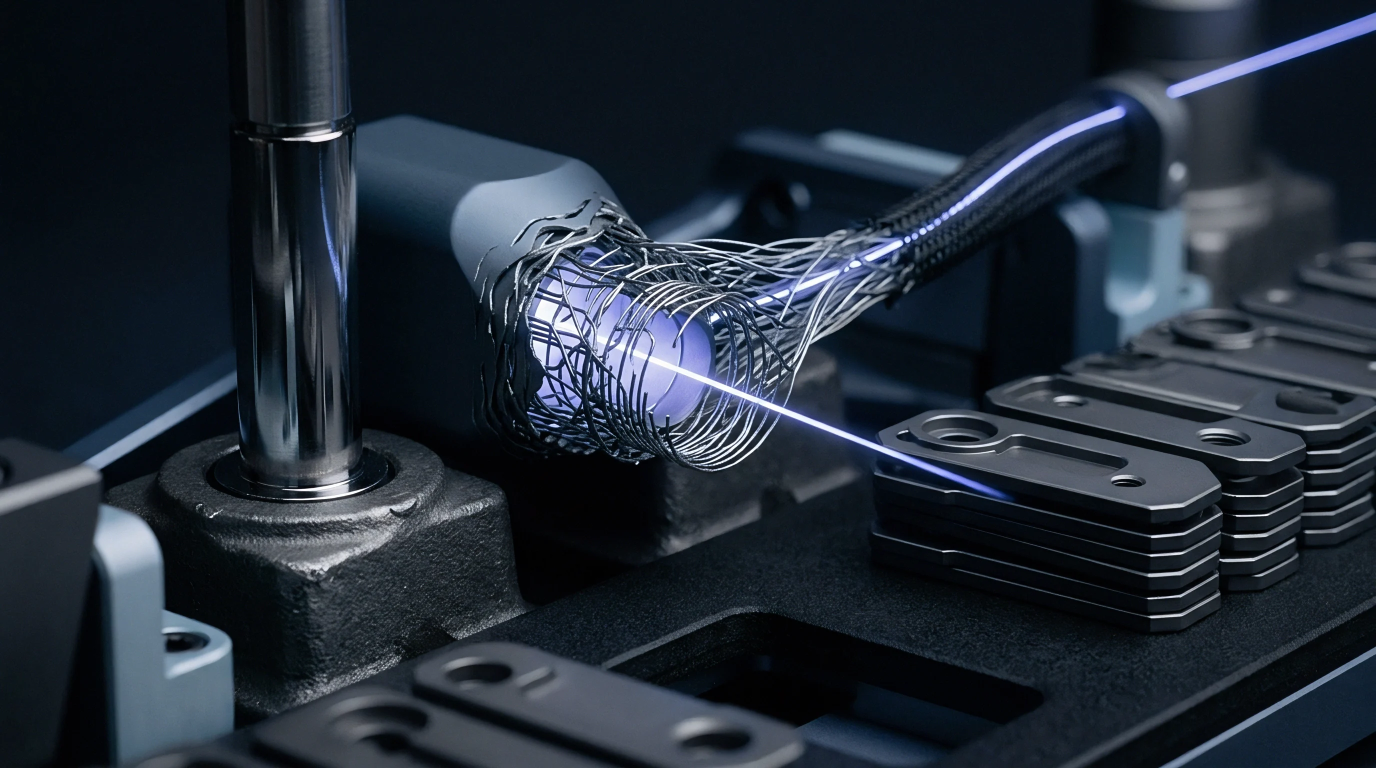
High Velocity Shear Testing and Standoff Metrology
Inspection criteria must pair high-velocity testing with precise geometric check. Solder joint standoff height governs the shear strain angle during board flex. Tighter standoffs concentrate bending displacements into a smaller vertical volume of solder, raising localized strain rates.
Automated optical inspection and three-dimensional X-ray metrology verify standoff heights stay within tolerance, confirming outer joints remain flexible enough to absorb transient shock.
Mixed-metallurgy assembly complicates screening protocols. When lines mount components with pre-attached SAC305 balls using low-temperature tin-bismuth paste, incomplete mixing often occurs. If peak reflow stays below 180°C, the SAC305 ball never melts, leaving a sharp boundary between the high-melting SAC sphere and the low-melting bismuth paste fillet.
Under shock loading, cracks run instantly along this unmelted seam.

Accelerometer Telemetry and Board Strain Thresholds
Instrumented drop testing verifies assembly survival under controlled acceleration pulses. Test vehicles fitted with high-speed tri-axial accelerometers and dynamic strain gauges undergo repeated drops per JEDEC standards. Piezoelectric accelerometers log peak deceleration, while digital telemetry records microstrain across vulnerable component corners at sampling rates up to one hundred kilohertz.
Setting allowable board strain limits protects low-temperature joints against premature cleavage. Peak strain during qualification must not exceed eight hundred microstrain for binary Sn42Bi58 assemblies, though modified ductile alloys can take up to twelve hundred microstrain under identical half-sine shock pulses. Sourcing specs without explicit dynamic strain limits leave hardware exposed to assembly process variations and unverified paste substitutions.
Inserting JEDEC JESD22-B117A condition C into master purchase specifications forces assembly houses to qualify high-velocity ball shear toughness before releasing low-temperature paste batches to active production lines.