Polymer Encapsulation Material Properties in Industrial Sensor Applications
Polymer encapsulation selection requires matching matrix CTE and modulus to die silicon to prevent parametric drift while maintaining moisture barrier limits.


Resin
Industrial transducer housings rely on engineered potting compounds to isolate silicon microstructures from chemical, thermal, and mechanical damage. Encapsulant layers prevent direct contact between corrosive ambient fluids and fragile interconnects. Choosing an unsuitable polymeric matrix compromises calibration stability over time and subjects wire bonds to severe mechanical shear.
When evaluating package durability, sourcing engineers must inspect the physical parameters of the uncured resin alongside its cured mechanical properties.
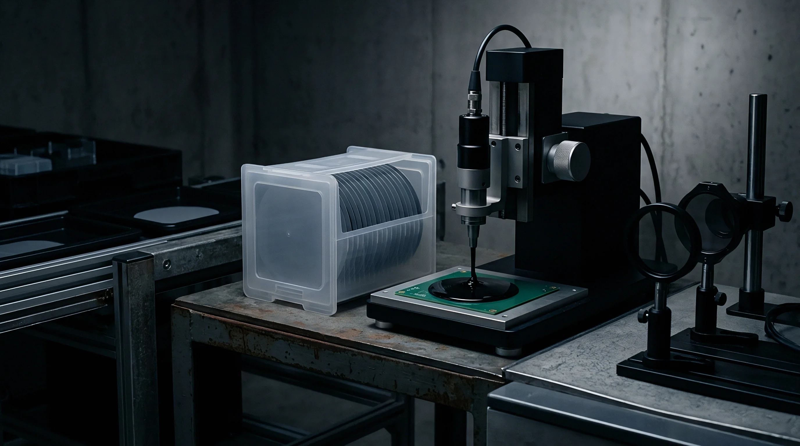
Polymer Chemistries in Industrial Sensor Packaging
Potting formulations divided into epoxies, silicones, polyurethanes, and fluorosilicones dictate the operational boundaries of field-deployed sensing elements. Epoxy resins form dense cross-linked networks that deliver tensile strengths exceeding 70 MPa alongside high resistance to aggressive industrial solvents. Their high glass transition temperature (Tg), often ranging from 120°C to 180°C, maintains mechanical rigidity under high ambient heat.
Fluorosilicones combine the low-temperature flexibility of traditional siloxanes with fuel and solvent resistance, making them suitable for automotive manifold pressure monitoring. Polyurethanes offer economical protection for washdown environments but suffer hydrolytic degradation above 85°C.
Viscosity directly governs gap-filling performance. Resins below 1,500 mPa·s flow into micro-gap cavities around surface-mount devices (SMD) without trapping bubbles, whereas high-viscosity thixotropic compounds stay where applied to form localized dams. The choice of application method determines whether the formulation needs multi-stage vacuum degassing to clear air voids prior to thermal curing, since peaks in the reflow profile promote void formation.
| Chemistry Class | Tg (°C) | CTE Below Tg (ppm/K) | Elastic Modulus (GPa) | Water Absorption (%) | Thermal Conductivity (W/m·K) |
|---|---|---|---|---|---|
| Cycloaliphatic Epoxy | 140 to 175 | 25 to 40 | 8.5 to 14.0 | 0.15 to 0.30 | 0.8 to 1.5 |
| Standard Bisphenol-A Epoxy | 110 to 135 | 45 to 65 | 3.0 to 6.5 | 0.35 to 0.60 | 0.2 to 0.5 |
| Two-Part Addition Silicone Gel | -65 to -45 | 250 to 350 | 0.001 to 0.010 | 0.05 to 0.12 | 0.15 to 0.30 |
| Filled Polyurethane Compound | -40 to 85 | 80 to 120 | 0.5 to 2.2 | 0.40 to 0.85 | 0.3 to 0.7 |
| Fluorosilicone Elastomer | -55 to -30 | 200 to 300 | 0.005 to 0.050 | 0.10 to 0.20 | 0.2 to 0.4 |
| Data measured at 23°C and 50% relative humidity per ASTM D696 and ASTM D570 standard test conditions. | |||||

Thermomechanical Properties across Operating Temperatures
Crossing the glass transition temperature shifts a polymer from a rigid matrix to a compliant elastic state. Below Tg, the material retains a low coefficient of thermal expansion (CTE) and a high storage modulus. Above Tg, CTE increases three- to fivefold while storage modulus drops by two orders of magnitude ~ a sudden transition that can crush gold wire bonds and create sharp thermal stress concentrations at component corners.
Thermal cycling induces mechanical warpage whenever the CTE of the encapsulant diverges from that of the substrate. Silicon dies expand at 2.6 ppm/K and FR4 substrates at 14 to 17 ppm/K, but unfilled potting resins can exceed 65 ppm/K. Loading the resin with fused silica fillers brings bulk expansion down to 18 ppm/K, easing the strain gradient across solder joints.
During thermal cycling between minus forty degrees Celsius and one hundred twenty-five degrees Celsius, mismatched expansion coefficients can shear surface-mount solder joints directly off their trace pads.
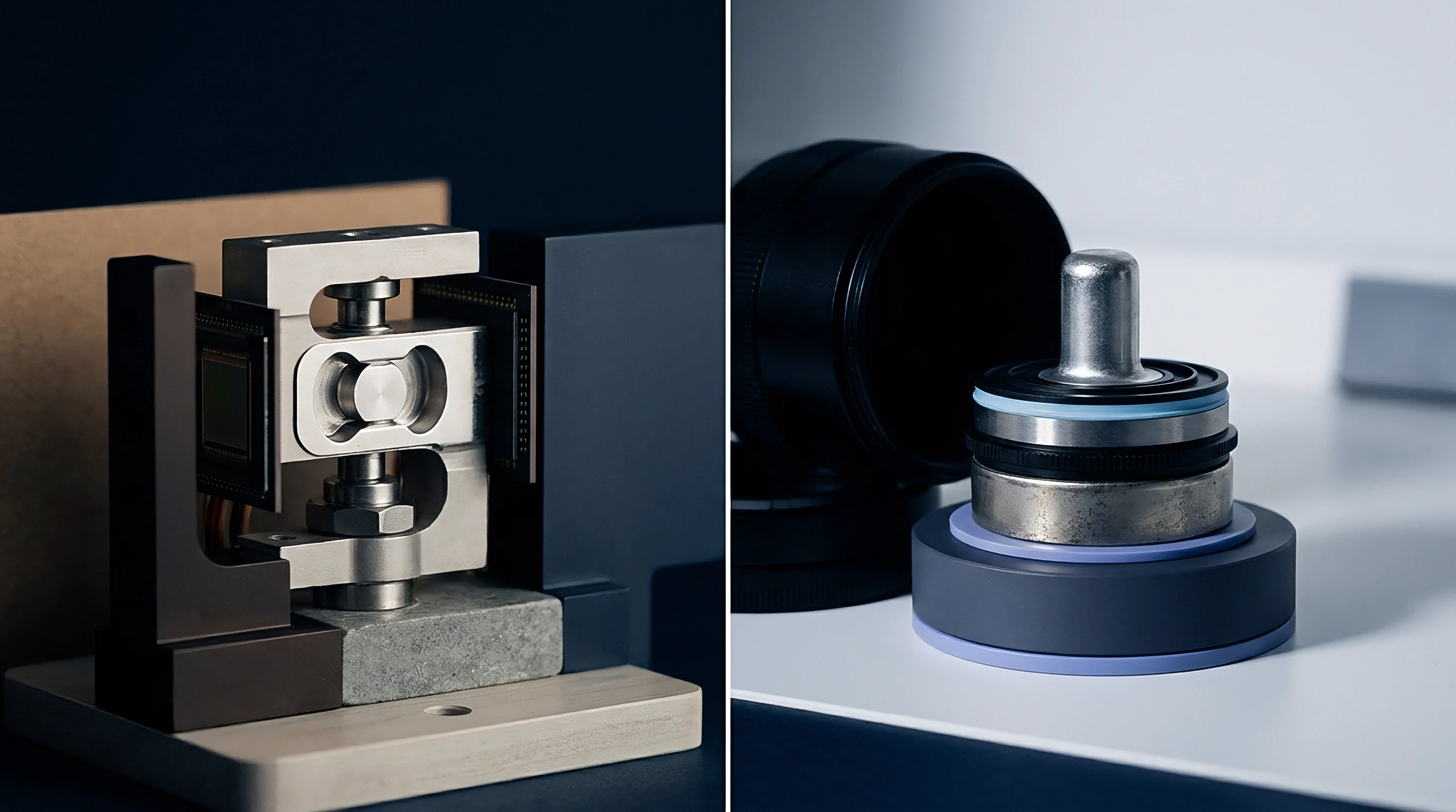

Stress
Mechanical forces passed from cured compounds into active silicon alter internal crystal lattices through piezoresistive coupling. The magnitude of this internal strain tracks resin shrinkage during polymerization and thermal cooling. Left uncompensated, this stress shifts the sensor’s zero-point output, producing measurement errors that host microcontrollers cannot readily filter out.

Die Distortion and Parametric Offset Drift
Volumetric shrinkage during cure generates substrate bending moments that unbalance Wheatstone bridges in micro-machined pressure diaphragms. Standard epoxies shrink 0.3% to 1.5% by volume as they polymerize. This compression applies isotropic force across encapsulated parts, distorting silicon microstructures and shifting trace resistance ~ an effect clearly seen when overmolding LGA-packaged precision pressure sensors with rigid materials.
Soft silicone gels limit force transfer by maintaining a low elastic modulus. Unfilled gel matrices remain below 10 MPa ~ compared to more than 8,000 MPa for rigid epoxies ~ allowing them to absorb dimensional shifts and cushion mechanical shock without transmitting compressive stress to the die. While gel encapsulation preserves diaphragm sensitivity, it demands a rigid outer housing to guard against fluid flow and mechanical puncture.
A rigid epoxy potting compound with a modulus of twelve gigapascals induces twenty-five megapascals of compressive stress on a uniaxially constrained silicon die during cool-down from one hundred fifty degrees Celsius.
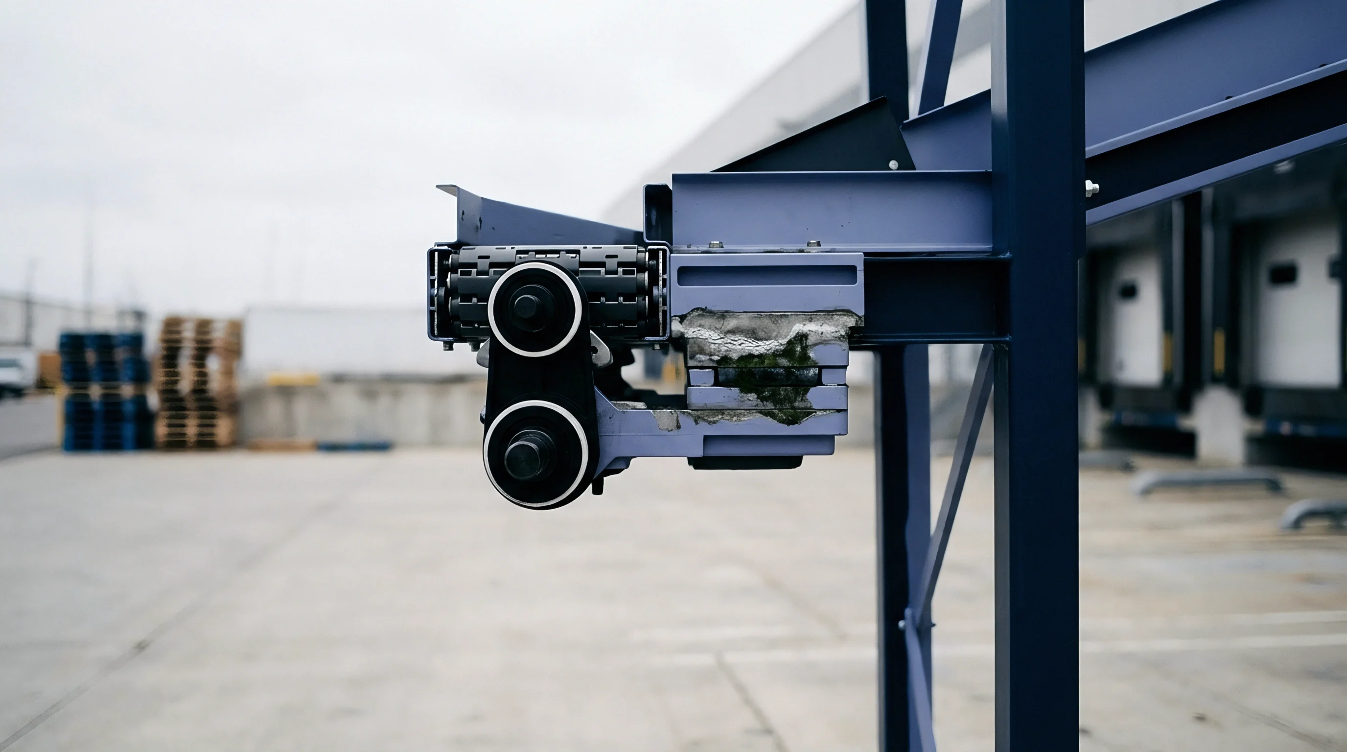
Piezoresistive Transduction Hysteresis Calculation
Piezoresistive coefficients of p-type silicon in the 100 plane govern voltage outputs when exposed to unequal biaxial compression. Consider a 3.0 mm by 3.0 mm by 0.4 mm MEMS pressure sensing die attached to an alumina substrate with conductive epoxy and encapsulated in a high-modulus mold compound. Assume the mold compound cures at 150°C and cools to 25°C room ambient.
The mold compound features an elastic modulus E of 12 GPa and an effective expansion coefficient delta-alpha of 15 ppm/K relative to silicon across the 125°C temperature difference.
Under uniaxially constrained conditions, the compressive stress sigma acting on the die surface scales according to:
sigma = (E delta-alpha delta-T) / (1 – nu)
Substituting a Poisson ratio nu of 0.28 yields:
sigma = (12,000 MPa 15e-6 / K 125 K) / (1 – 0.28) = 31.25 MPa
Although silicon dies fracture primarily under tension, an applied compressive stress of 31.25 MPa alters the resistance of Wheatstone bridge piezoresistors. Given a longitudinal piezoresistive coefficient pi_44 of 72e-11 Pa^-1, the resulting fractional change in resistance delta-R/R follows:
delta-R/R = 0.5 pi_44 sigma = 0.5 (72e-11 Pa^-1) (31.25e6 Pa) = 0.01125
A 1.125% change in baseline resistance produces a 22.5 mV zero offset on a 2.0 V full-scale bridge output, consuming 11.25% of the analog front-end dynamic range. Across operating swings from -40°C to +125°C, polymer thermal hysteresis prevents the zero-point voltage from recovering its original baseline, locking in a permanent offset error.
Failure modes inside encapsulated packages stem directly from severe mechanical stress concentrations across internal material interfaces:
- Die Passivation Cracking occurs when severe shear gradients across thermal boundaries break protective silicon nitride coatings.
- Wire Bond Fatigue shears gold or aluminum wedge bonds at the bond pad boundary after repeated power cycles.
- Delamination at Die Attach isolates the silicon substrate thermally, causing rapid local heating and zero-point calibration shifts.
- Piezoresistive Zero Shift shifts bridge outputs past the dynamic range of internal analog front-end gain stages.
Selecting soft silicone gels over rigid epoxy compounds preserves micro-machined diaphragm sensitivity when ambient operating temperatures fluctuate widely.


Moisture
Atmospheric moisture diffuses through organic encapsulants, shifting internal bulk resistivity and causing physical swelling. Liquid water ingress degrades die passivations and triggers galvanic corrosion on aluminum bond pads. Permeation rates depend on polymer packing density, temperature, and local vapor pressure gradients across the barrier.
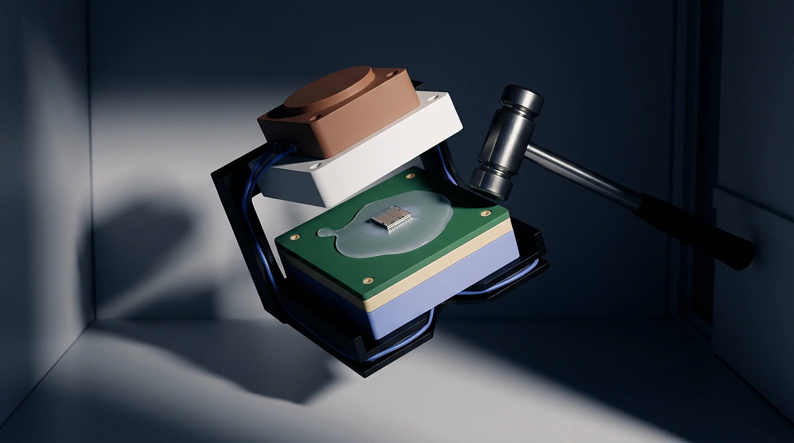
Ingress Kinetics and Water Vapor Transmission
Fickian diffusion models describe how moisture moves through polymer barriers to bare silicon over time. The water vapor transmission rate (WVTR) measures this mass flow through a specific encapsulant thickness: polyurethanes exceed 25 g/m²·day at 38°C and 90% relative humidity, while dense epoxies remain below 1.5 g/m²·day. Moisture ingress raises the matrix dielectric constant and introduces parasitic capacitance between adjacent conductors, while trace ionic impurities accelerate leadframe degradation.
| MSL Rating | Floor Life (Time at <=30°C / 60% RH) | Bake Requirement Before Assembly | Volumetric Swelling Range (%) |
|---|---|---|---|
| MSL 1 | Unlimited | None required prior to reflow | 0.02 to 0.05 |
| MSL 2 | 1 Year | Bake at 125°C for 16 hours if expired | 0.05 to 0.12 |
| MSL 3 | 168 Hours | Bake at 125°C for 24 hours if expired | 0.12 to 0.35 |
| MSL 4 | 72 Hours | Bake at 125°C for 48 hours if expired | 0.30 to 0.55 |
| MSL 5 | 48 Hours | Bake at 125°C for 48 hours if expired | 0.50 to 0.85 |
Reflow Sensitivity and Delamination Protocols
Tracking floor life controls moisture uptake before reflow soldering spikes vaporize trapped water. During lead-free profiles peaking at 260°C, rapid steam expansion generates internal pressure that exceeds resin adhesion, driving interface separation commonly known as popcorning. Thermal baking removes this absorbed water prior to assembly.
JEDEC J-STD-033 Clause 4.2 mandates floor-life reset baking at one hundred twenty-five degrees Celsius for twenty-four hours when exposed duration exceeds allowable limits.
Receiving inspection operations must verify component packaging integrity to prevent assembly line defects. Incoming inspection routines require checking seal integrity on moisture barrier bags before releasing parts to SMT lines. The following verification steps protect factory floor yields:
- Humidity Indicator Verification confirms that the enclosed desiccant maintained internal bag relative humidity below ten percent during transit.
- Bag Seal Inspection checks heat-seal seam integrity for pinhole ruptures or vacuum loss prior to warehouse storage.
- Bake Record Audit verifies that factory floor baking cycles matched specified temperature and duration parameters for expired lots.
- Weight Change Measurement quantifies moisture absorption percentage by measuring component mass before and after thermal baking.
Incorporating IPC J-STD-020 Clause 5.4 into procurement quality agreements obligates suppliers to deliver all Level 3 packaged sensor units in sealed moisture barrier bags with humidity indicator cards reading below ten percent.

Bus
Digital communication backplanes integrated inside encapsulated sensor modules suffer physical signal degradation from potting dielectric properties. The presence of a high-permittivity polymer surrounding unshielded PCB traces increases total trace capacitance to ground. High capacitance rounds off signal edge transitions, introducing timing jitter and distorting square waves on high-speed serial lines.
Does Encapsulation Dielectric Constant Shift High Speed Bus Capacitance?
Potting media surrounding internal printed circuit traces increase parasitic capacitance relative to open air. Standard FR4 substrate dielectric constant sits near 4.4, while air measures 1.0. Epoxy potting materials possess dielectric constants between 3.5 and 5.5, while high-k filled formulations reach 9.0.
Encapsulating an unshielded signal trace increases line capacitance by 30% to 75%, shifting bus RC time constants.
For an I2C communication bus operating in Fast-Mode Plus at 1.0 MHz, the maximum allowable bus capacitance totals 550 pF. Standard pull-up resistors sized at 2.2 kΩ combined with an encapsulated trace capacitance of 400 pF produce a bus rise time t_r calculated by:
t_r = 0.8473 R_pullup C_bus = 0.8473 (2200 Ω) (400e-12 F) = 745.6 ns
A rise time of 745.6 ns violates the 120 ns maximum allowed under the I2C Fast-Mode Plus specification. As a result, the host fails to detect valid logic high levels and registers framing errors. Adding ground shielding around sensitive traces helps isolate them from these dielectric-driven capacitance shifts and ambient noise spikes.

Interface Selection and Signal Integrity in Potting
Architectural choices between differential RS-485, three-wire SPI, two-wire I2C, and single-wire IO-Link determine physical noise margins. Encapsulated modules using high-impedance analog outputs suffer voltage drops from moisture-induced leakage currents across potting interfaces. Differential digital interfaces resist parasitic capacitance shifts better than single-ended lines.
SPI buses require lower series termination resistance when encapsulated to maintain fast clock transition edges above 10 MHz.
Validation of an encapsulated sensor module across manufacturing stages follows a strict sequence:
- Sample raw unencapsulated sensor bridge voltages across five baseline operating temperatures in a environmental chamber.
- Apply silicone gel potting inside the stainless steel housing and cure according to manufacturer thermal ramp profiles.
- Perform a 400 kHz I2C bus read sequence to confirm register communication and log zero-offset voltage shift.
- Subject the assembled module to one thousand thermal shock cycles from minus forty to one hundred twenty-five degrees Celsius.
- Measure signal trace rise time and bus capacitance on an oscilloscope to verify line driver timing parameters stay within specified thresholds.
Thick potting layers around unshielded signal traces increase parasitic line capacitance and reduce maximum communication bus clock frequencies.
Unaccounted sensor zero drift often stems from uncompensated epoxy cure stress on internal silicon elements rather than customer soldering thermal profiles.


Procurement
Commercial pricing structures for identical sensing silicon vary across five order magnitude increments based on protective outer housings. A bare silicon pressure transducer die costs less than one dollar at high volumes. Mounting that same die into a surface-mount DFN package elevates the price to three dollars.
Overmolding the DFN into an IP67-rated cabled stainless steel probe pushes the final unit cost past forty dollars. Sourcing teams analyze these price steps against assembly yield loss and warranty exposure.

Packaging Variant Price Ladders
Raw silicon dies purchased on wafer tape command low unit costs but require micro-assembly capital equipment. Surface-mount packages allow standard high-speed pick-and-place placement but demand careful land-pattern design to avoid solder joint bridging under thick conformal coatings. Module-on-board variants integrate discrete passive components, internal regulators, and pre-programmed microcontrollers inside a single overmolded block, transferring integration labor from the buyer to the package vendor.
Trapped air bubbles reduce yields during potting, while custom molds require upfront capital tooling expenditure.
| Package Variant Form | Unit Price at 10k Volume (USD) | Minimum Order Quantity (Units) | Yield Loss Percentage (%) | Factory NRE Tooling Cost (USD) |
|---|---|---|---|---|
| Bare Silicon Die on Tape | 0.85 | 50,000 | 4.5 to 8.0 | 0 |
| SMD DFN Plastic Package | 2.40 | 5,000 | 0.5 to 1.2 | 0 |
| Gel-Filled Metal Can LGA | 5.80 | 1,000 | 1.0 to 2.5 | 2,500 |
| Overmolded PCB Module | 14.50 | 500 | 1.5 to 3.0 | 12,000 |
| IP68 Stainless Steel Cabled Unit | 48.00 | 100 | 0.2 to 0.8 | 25,000 |
Make or Buy Thresholds in Potting Assembly
Capital expenditures for vacuum degassing equipment, automated epoxy dispensing heads, and curing ovens set the volume break-even point for in-house potting operations. Dispensing equipment capable of maintaining +/- 1% volumetric mixing ratios on two-part epoxies costs approximately $85,000. Automated inline vacuum chambers add another $60,000.
A buyer processing fewer than 20,000 units per year achieves lower landed costs by purchasing fully encapsulated module assemblies directly from component vendors.
Selecting package variants during technical RFQ reviews requires balancing mechanical protection against long-term maintenance costs. Engineering teams evaluate key operational factors:
- Operating Media Compatibility defines whether low-cost polyurethanes suffice or aggressive solvents demand high-fluorine fluorosilicones.
- Thermal Cycle Limits establish required coefficient of thermal expansion matching between substrate material and encapsulation matrix.
- Board Space Footprint determines if an embedded surface-mount DFN component fits or external cabled housings are required.
- Firmware Compensation Needs clarify whether raw analog millivolt outputs or factory-calibrated digital I2C variants lower total project cost.
Whether long-term material hydrolytic degradation in harsh subterranean chemical monitoring justifies the upfront capital expense of glass-to-metal hermetic seals over high-grade fluorosilicone potting remains an open operational question.