Managing Board Stray Capacitance in Fast Mode plus Bus Integration
Managing Fast Mode Plus stray capacitance requires low capacitance trace layout active pull up current sources and bus buffers to meet 120 ns rise times
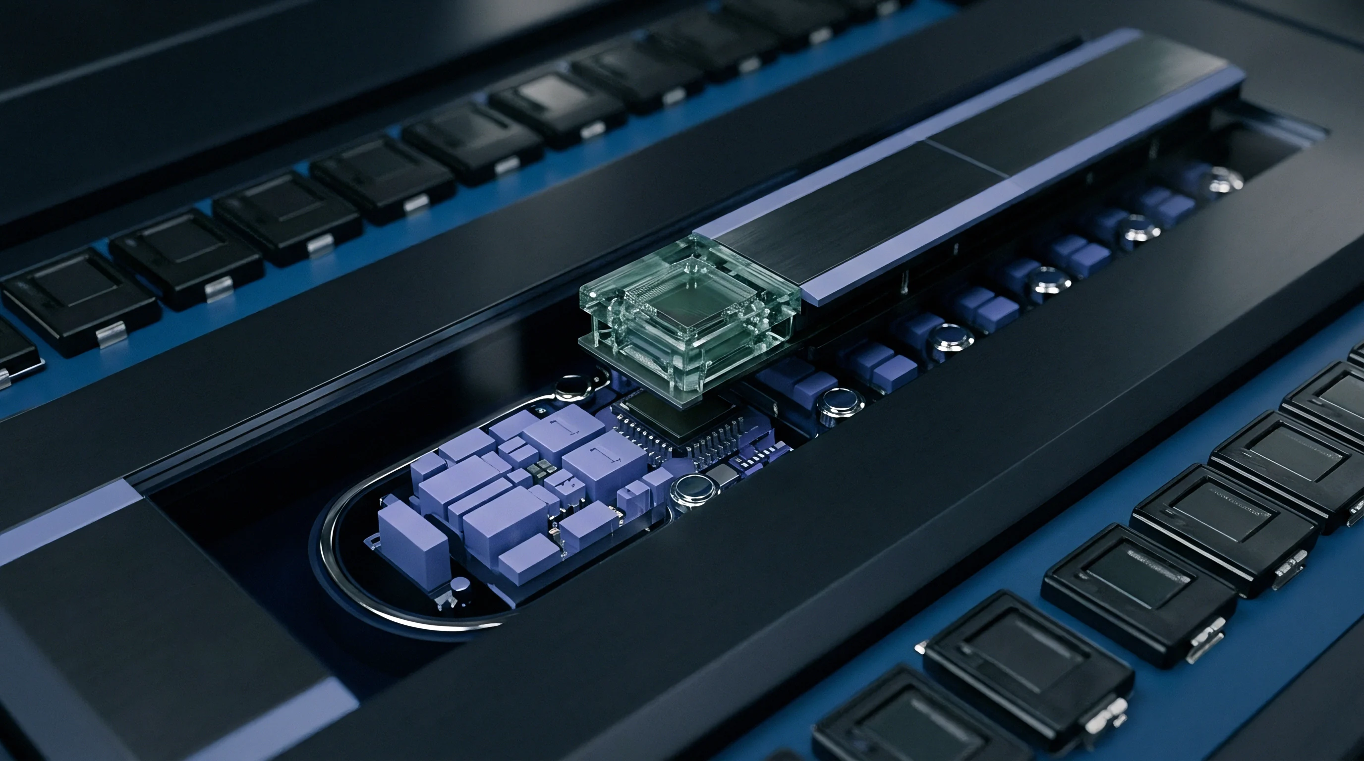

Copper
Layout choices on a printed circuit board directly govern the parasitic loading on serial data and clock lines. Distributed trace capacitance forms a continuous RC filter with the pull-up resistance, rounding off rising edges and shifting signal timing. Controlling trace dimensions, stackup geometry, and copper ground plane clearances is essential to manage this built-up capacitance.

Trace Geometry and Dielectric Layering
External microstrip traces over FR-4 substrates add roughly 1.2 pF to 1.8 pF of parasitic load per inch. The precise figure hinges on trace width, copper thickness, and height above the reference plane. Burying conductors as striplines between two ground planes increases this capacitance by 40 to 60 percent because the field distributes across both planes.
Narrowing traces from 0.20 mm down to 0.10 mm lowers line capacitance, though ultra-narrow routing brings higher series resistance and looser manufacturing etching tolerances.
Ground planes draw and concentrate electric fields.
Running a solid ground plane directly under serial traces maximizes capacitive coupling. Clearing reference copper beneath fast signals ~ ground pullback ~ cuts local stray loading by up to 0.6 pF per land pad. High-density interconnect layouts transitioning across multiple layers add further parasitic nodes at microvia structures.
- Microstrip signal traces add roughly 1.5 pF per inch when routed over standard FR-4 layers with 0.1 mm spacing.
- Surface mount land pads contribute 0.5 pF to 2.1 pF apiece, depending on pad footprint, copper weight, and distance to the reference ground.
- Layer transition vias insert about 0.4 pF per pass through multi-layer PCB stackups due to barrel surface area and ground clearance voids.
- Tuning component footprints such as TVS diode array pads add 1.5 pF to 5.0 pF of stray capacitance right across signal nodes.
Stackup selection dictates total bus parasitics long before parts are placed. Thinner prepreg brings ground planes closer to signal traces, sharply raising capacitance and slowing signal edges.
At 1000 kHz Fast Mode Plus clock frequencies, board stray capacitance above 150 pF forces pull-up resistance below 260 ohms to satisfy the 120 ns maximum rise time specification.
Ignoring dielectric thickness tolerances and trace spacing in dense layouts causes unpredictable rise times, corrupted frames, and outright communication failure when bringing up multi-node Fast Mode Plus buses.


Silicon
IC packaging introduces pin capacitance and bond wire inductance that stack onto external board parasitics. Internal silicon features, ESD protection diodes, and lead frame geometry define a baseline load for every node on the bus. Selecting sensor variants means accounting for internal package parasitics right alongside PCB land pattern loads.
Package Variants and Pin Capacitance
IC design relies on protective ESD rings to isolate I/O structures, which adds parasitic junction capacitance. Internal ESD diodes add 1.5 pF to 4.0 pF per pin. In traditional dual-in-line or Small Outline Integrated Circuit (SOIC) packages, bond wires and lead frame contacts introduce secondary series inductance and pin-to-pin coupling, increasing total internal loading with higher pin counts.
Bond wires introduce additional series inductance.
Wafer-Level Chip-Scale Packages (WLCSP) and Quad Flat No-Lead (QFN) footprints strip away lead frames, dropping package capacitance down to 1.5 pF per pin. Plastic molded packages with long leads retain higher pin parasitics that drag down node transitions. Networks aggregating twelve to sixteen slave devices on a single Fast Mode Plus trunk accumulate over 50 pF in package capacitance alone, before adding any PCB trace routing.
| Package Type | Nominal Pin Capacitance | Land Pad Capacitance | Total Per-Node Load |
|---|---|---|---|
| WLCSP-6 (0.4mm pitch) | 1.8 pF | 0.3 pF | 2.1 pF |
| DFN-8 (2x2mm) | 2.5 pF | 0.6 pF | 3.1 pF |
| QFN-16 (3x3mm) | 3.2 pF | 0.9 pF | 4.1 pF |
| SOIC-8 (1.27mm pitch) | 5.5 pF | 1.8 pF | 7.3 pF |
| Cabled Module Assembly | 12.0 pF | 4.5 pF | 16.5 pF |
Larger footprints simplify manufacturing but carry higher capacitive penalties. Land pads for SOIC-8 packages double local copper capacitance compared to DFN pads. These package-level differences dictate how much driver capacity is required to maintain 1 MHz clock operation.
Quoted package capacitance values apply only to isolated test fixtures operating without solder paste, board traces, or secondary protection components.


Current
Pull-up resistors and active drive circuits establish the charging rate for low-to-high line transitions. Passive pull-ups follow exponential RC charging curves, with rise times scaling directly with net capacitance. Fast Mode Plus bus designs rely on higher sink currents to accommodate smaller pull-up resistor values or active current sources.
Active Drivers and Dynamic Pull-Up Sizing
Standard open-drain drivers rely on passive pull-ups to pull line voltage toward supply rails. Under the NXP UM10204 Fast Mode Plus specification, the maximum allowed rise time from 0.3 VDD to 0.7 VDD is 120 ns. The exponential charging equation gives a rise time constant of 0.8473 times pull-up resistance times total bus capacitance.
For a bus carrying 300 pF of total stray load, the maximum passive pull-up resistance works out to 120 ns divided by (0.8473 × 300 pF), or 472 ohms.
Active drivers sink current to pull bus voltages low.
Sinking current through a 472 ohm resistor at 3.3 V forces the drive transistor to pull 6.15 mA while keeping low-level output voltage under 0.4 V. Standard I2C devices specify a maximum low-level sink current of only 3 mA, making passive pull-ups impossible for Fast Mode Plus at a 300 pF bus load. Fast Mode Plus drivers specify 20 mA sink capability at 0.4 V, allowing pull-up resistance down to 145 ohms.
| Speed Mode | Max Clock Rate | Max Bus Load | Max Rise Time | Max Fall Time | Min Sink Current |
|---|---|---|---|---|---|
| Standard Mode | 100 kHz | 400 pF | 1000 ns | 300 ns | 3 mA |
| Fast Mode | 400 kHz | 400 pF | 300 ns | 300 ns | 3 mA |
| Fast Mode Plus | 1000 kHz | 550 pF | 120 ns | 120 ns | 20 mA |
Active current sources replace fixed resistors with constant-current charging circuits to accelerate rising edges.
- Passive pull-up resistors suit low node counts where total bus capacitance stays below 150 pF.
- Active current sources become necessary when bus capacitance ranges from 150 pF to 400 pF, preventing excessive static power drain.
- Switched pull-up accelerators kick in briefly during rising transitions when total stray load exceeds 400 pF across long backplanes.
- Bidirectional bus repeaters isolate heavy physical segments into separate 100 pF load domains as bus length grows.
Dynamic current injection charges bus capacitance linearly instead of exponentially. Constant-current charging reaches the logic-high threshold in a fraction of the time taken by passive resistors. This faster charge time allows operation up to the maximum 550 pF specification limit without exceeding output sink current limits.
Splitting a heavy Fast Mode Plus trunk into isolated sub-segments with bidirectional bus buffers reduces effective node capacitance back within single-driver limits.
Placing strong pull-up devices right next to the heaviest capacitive load helps preserve sharp signal edges across all slave nodes.

Transit
Signal propagation along capacitive lines directly alters rise times, fall times, and data setup margins. As total capacitive loading increases, rising edges flatten, shrinking the window where logic levels remain stable before clock transitions. System integrators must evaluate full timing budgets to guarantee reliable transmission across operating temperatures.
Where Does High Stray Capacitance Degrade Fast Mode plus Timing Budgets?
Elevated bus loading stretches signal edges past logic thresholds, narrowing the valid data sample window before clock transitions. Fast Mode Plus requires a minimum data setup time of 50 ns and a data hold time between 0 ns and 70 ns. Slower rising edges from high stray capacitance delay when line voltage crosses the logic-high threshold, consuming setup margin.
Receiver noise margins degrade quickly under heavy loading.
If rise time stretches from 120 ns to 200 ns due to unexpected trace capacitance, data setup time drops below zero and corrupts incoming bits at the receiver. Host microcontrollers can adjust internal timing registers to lengthen SCL low intervals, accommodating slower edges at the cost of overall bus throughput.
- Measure exact rising edge duration from 30 percent to 70 percent supply voltage using a high-bandwidth oscilloscope.
- Calculate the added setup delay introduced by slow transitions across the node network.
- Increase host peripheral SCL high-period clock cycles to maintain a minimum 260 nanosecond pulse width.
- Adjust internal data hold delay registers to prevent false start or stop condition triggers during transitions.
Clock stretching happens when slave devices hold SCL low to delay host clock generation during processing. High capacitive loading worsens this by slowing signal recovery once the slave releases the line. Excessive edge delays can trigger driver timeouts in host firmware, forcing full bus resets.
Compliance with the UM10204 Fast Mode Plus bus specification mandates a maximum 120 ns rise time and 120 ns fall time across the full 400 pF maximum bus load.
Section 6.2 of the NXP UM10204 Fast Mode Plus Bus Specification mandates bus buffering whenever line capacitance exceeds 550 pF, forcing physical segmentation in compliant designs.
Audit
Validating physical bus lines requires precise measurement to separate trace capacitance from component pin parasitics. Standard oscilloscope probes insert 10 pF to 15 pF of parallel load, masking real line behavior during testing. Bench evaluation requires low-capacitance active probes or direct vector network analysis to isolate parasitic terms.
Bench Instrumentation and Parasitic Extraction
Time-domain reflectometry and high-frequency LCR meters isolate capacitance across individual traces and land patterns. Measuring an unpopulated board establishes baseline PCB stray capacitance, after which populating sensor nodes sequentially reveals the exact capacitive load added by each package variant.
Standard scope probes add loading to delicate signal lines.
Active FET probes present under 0.8 pF of input capacitance, preventing probe loading from distorting observed rise times. Standard passive probes drag down signal edges, creating false non-compliance readings. Logic analyzers monitoring bus traffic can catch setup violations and timing jitter during multi-master arbitration.
- Active FET probe selection eliminates measurement loading by keeping input capacitance under 0.8 pF during evaluation.
- In-circuit LCR evaluation quantifies net line capacitance before SMT assembly to establish baseline trace values.
- Logic threshold logging captures voltage transition levels to verify noise margin clearance under heavy dynamic loads.
- Signal edge rate analysis checks rising edge linearity to catch resonant ringing caused by trace stubs.
Protocol analyzers record framing errors under worst-case capacitive loading. Combining high-temperature testing with maximum bus loading exposes parametric timing failures driven by dielectric thermal expansion and reduced carrier mobility.
Whether embedded microcontrollers can dynamically adjust driver slew rates to compensate for temperature-dependent dielectric shifts remains an open engineering question.
Expense
Mitigating stray capacitance impacts both direct component cost and overall bill-of-materials complexity. Active bus buffers or higher-performance drive solutions add unit cost, but they save board real estate and reduce bring-up effort. Sourcing decisions balance piece price against assembly yield and re-spin costs.
Variant Pricing and Integration Trade-Offs
Selecting sensors with integrated bus buffers increases unit purchase price but simplifies layout requirements. Adding discrete accelerators or bidirectional buffers adds component count and consumes board area. PCB stackup adjustments ~ like adding dielectric layers or specifying tight impedance controls ~ raise bare-board fabrication costs across volume runs.
Unit component costs scale directly with design complexity.
Board revisions quickly consume engineering design budgets.
A sensor die in an SOIC-8 package carries a low procurement cost, but its high stray capacitance often forces the addition of buffer ICs. Sourcing the same die in a WLCSP package drops parasitic loading enough to allow direct bus coupling without external drivers. Evaluating true BOM impact means weighing component piece price against board space penalties and firmware risks.
| Strategy Option | Unit Component Cost Adder | Added PCB Area | Engineering Bring-Up Time | System Reliability Rating |
|---|---|---|---|---|
| Low-Value Passive Resistor Array | $0.02 | 4 mm² | 12 Hours | Medium (High Power Drain) |
| Active Current Source Acceleration IC | $0.28 | 9 mm² | 24 Hours | High (Clean Edges) |
| Bidirectional Bus Buffer IC | $0.55 | 16 mm² | 40 Hours | High (Isolates Capacitance) |
| Integrated Buffered Sensor Variant | $0.85 | 0 mm² | 8 Hours | Very High (Pre-Qualified) |
Redesigning PCB stackups late in product development causes costly engineering change orders and delays production. Sourcing active accelerators upfront stabilizes signal integrity on dense backplanes, avoiding last-minute firmware workarounds.
Selecting a sensor variant with integrated bus buffering adds upfront package cost but eliminates discrete level-shifters and passive arrays across multi-node board architectures.
Evaluating total landed cost on high-density boards shows that paying a premium for buffered sensor packages yields net savings once assembly yield loss and engineering bring-up hours are factored into high-volume budgets.