
Silicon Substrate Stress Mitigation for Piezoresistive MEMS Transducers
Mounting piezoresistive dies on borosilicate glass pedestals with low-modulus gel encapsulation isolates packaging strain and reduces zero-offset drift.
Mounting piezoresistive dies on borosilicate glass pedestals with low-modulus gel encapsulation isolates packaging strain and reduces zero-offset drift.
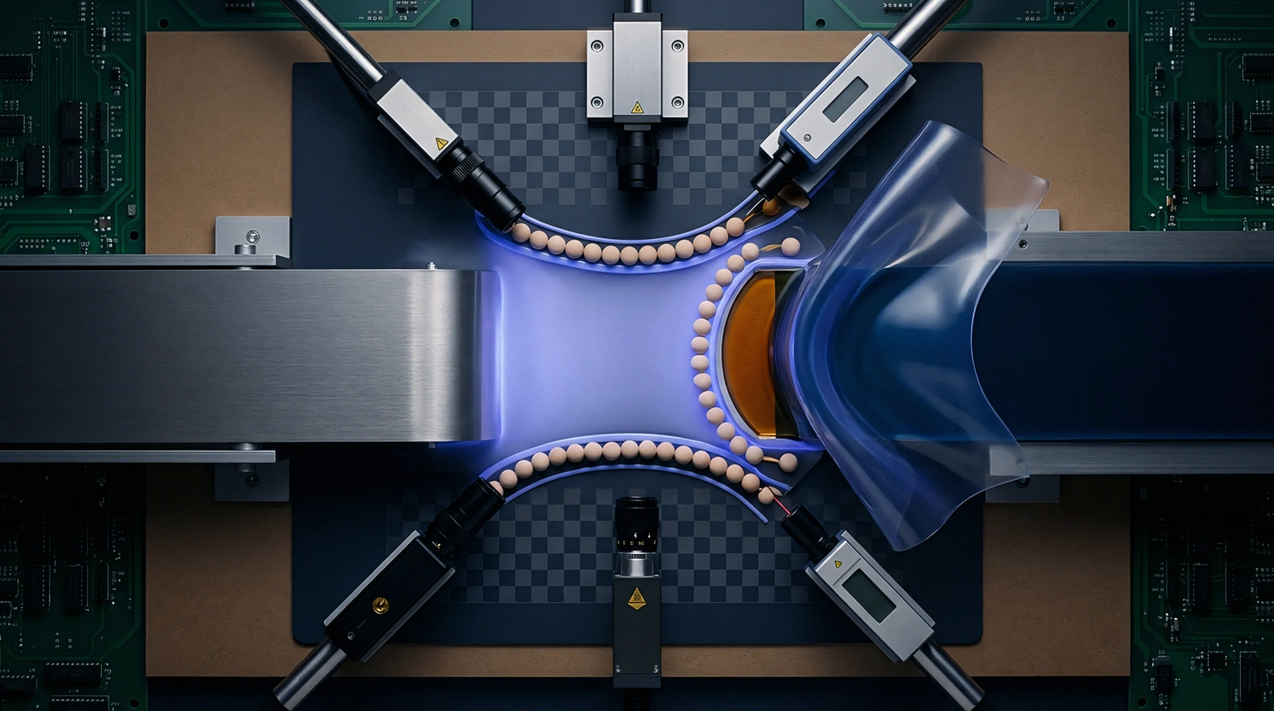
Verify ICT and depaneling strain rates below IPC/JEDEC-9704 dynamic limits using three-wire triaxial rosettes placed within two millimeters of package corners.
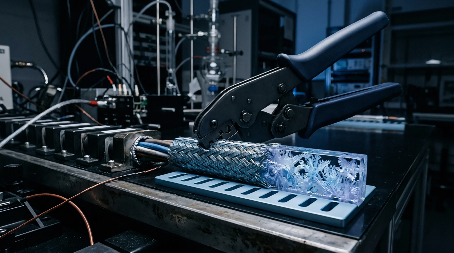
Asymmetric clamping torque on pressure port glands induces anisotropic diaphragm strain, driving piezoresistive zero shift that digital calibration cannot isolate.
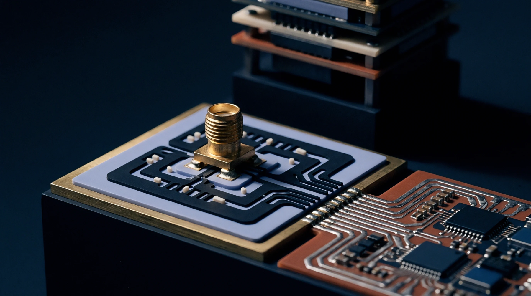
Precision PCB stress relief requires milled isolation slots around sensitive packages alongside symmetrical non-solder-mask-defined land patterns.

Micro-anchor decoupling isolates acoustic energy and relieves packaging strain, preserving quality factors over 100,000 and sub-ppm frequency stability.

Packaging mold shrinkage and board reflow solder strain alter silicon bandgap voltages via piezoresistive coupling, demanding compliant leads or ceramic packages.
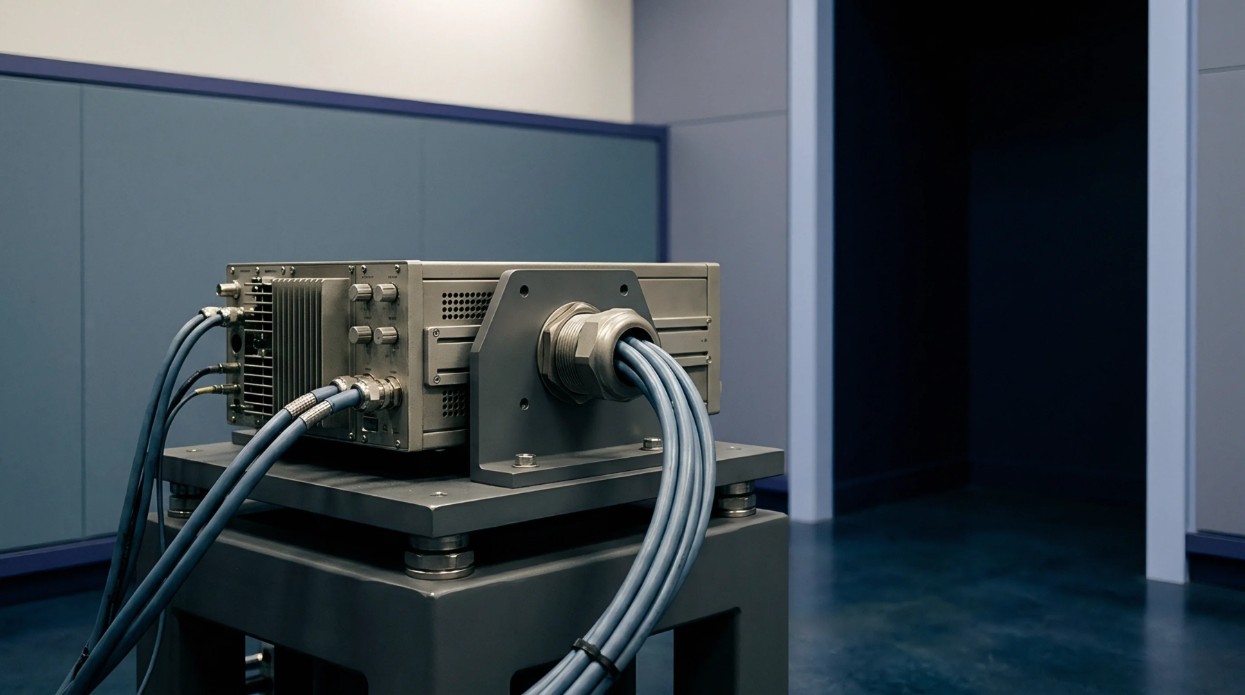
Milled PCB isolation slots and compliant leaded packages attenuate board-level thermal gradient strain to preserve 24-bit converter offset accuracy.
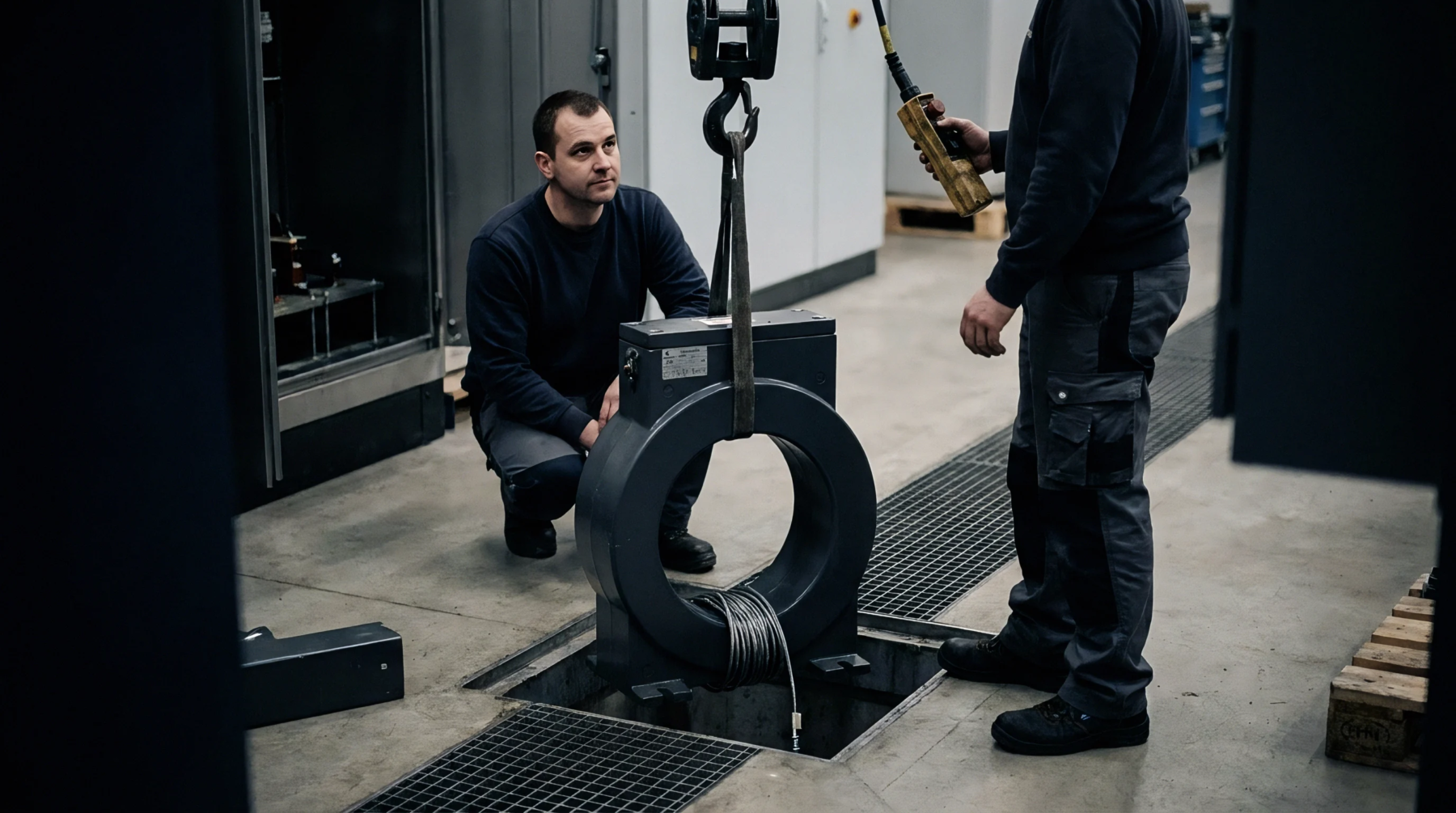
Precision voltage references demand symmetric copper lands, isolation slots, and convective shielding to suppress piezoresistive and thermoelectric drift.

Minimizing reference drift requires non-solder-mask-defined pads, compliant gull-wing packages, and perimeter routed slots to isolate circuit board strain.
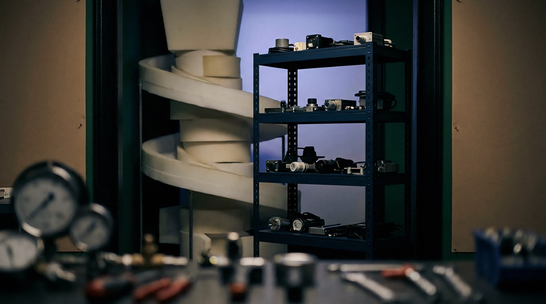
Characterizing packaging strain relaxation under forced convection isolates thermal boundary layer stripping from fluid line pressure to secure true sensor accuracy.
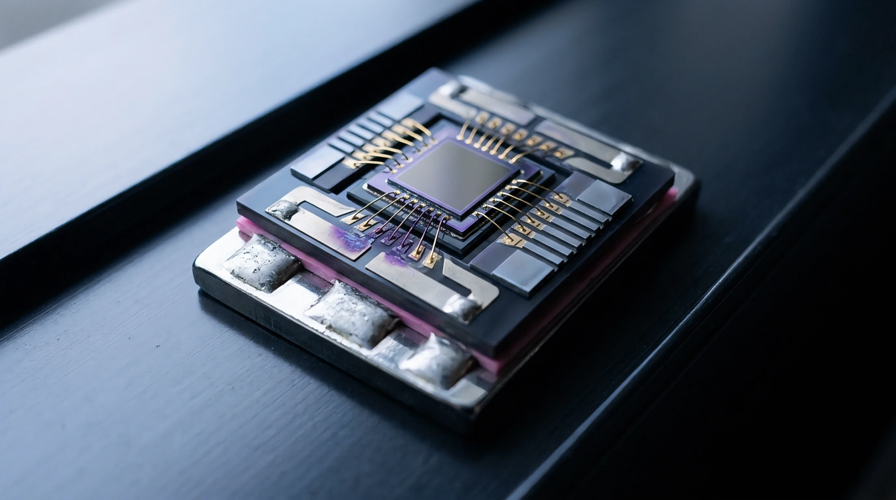
Sensor package selection fixes mechanical strain, driver stability, and break-even volumes before procurement issues purchase orders for alternative parts.
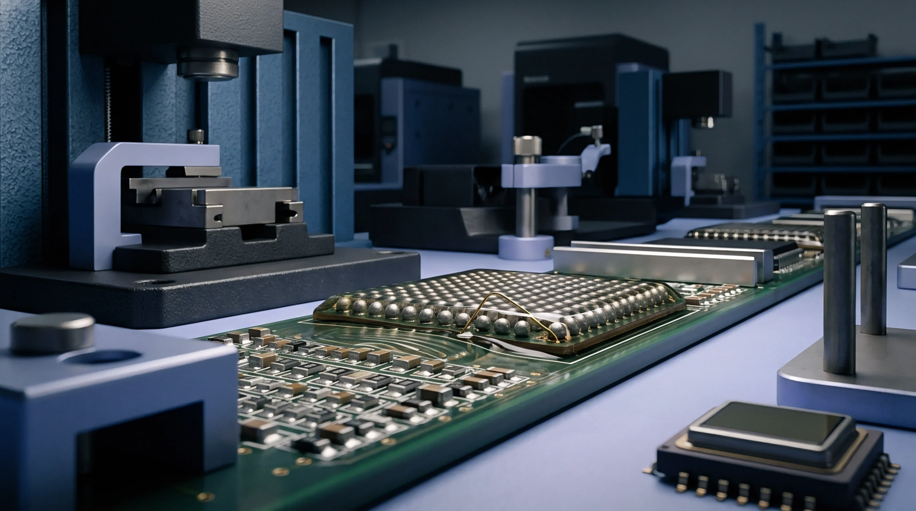
Triaxial strain rosette signal acquisition during depaneling audits requires simultaneous 50 kHz sampling and 10 kHz anti-aliasing filtering to capture true strain peaks.
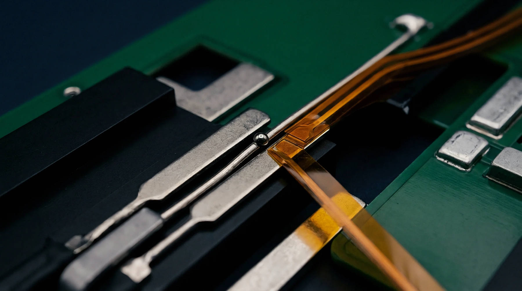
Dynamic PCB thermal gradients cause substrate flexing that alters converter resistor ladder ratios via piezoresistive strain, driving gain drift.
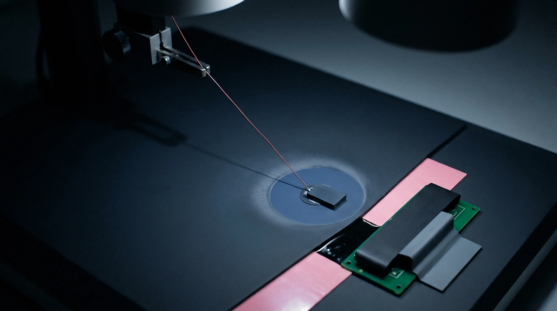
PCB deformation transfers mechanical strain through solder joints into surface-mount sensor dies, causing severe zero drift that requires package isolation or layout slots.
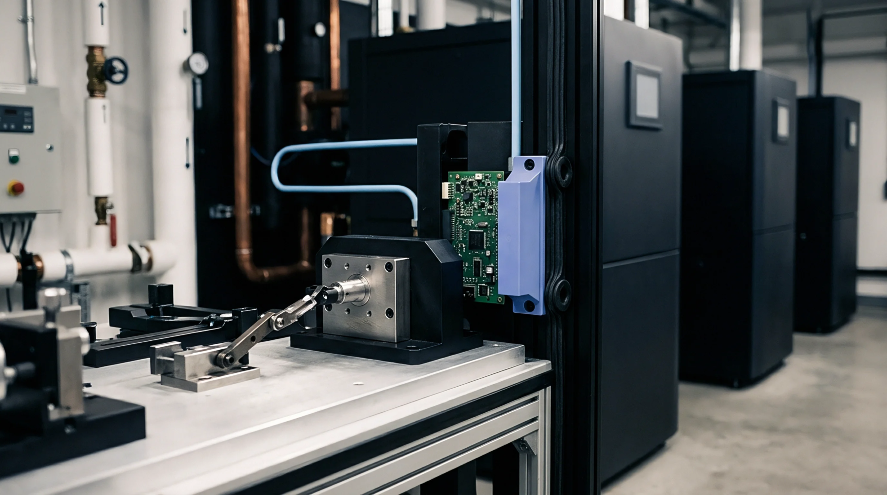
Board flexure transfers shear strain through solder joints into silicon dies, shifting zero-point offsets; isolate footprints using slots or diagonal placement.
Expertise is a utility, not a secret. sentiention™ publishes its working knowledge as open reference: intelligence layer covering the materials it sources, the markets it enters, and the reference that serves both.