Differential Trace Discontinuity Effects in High Speed Sensor Packaging
Differential trace discontinuities in high-speed sensor packages generate common-mode noise and timing jitter that require trace compensation and ground shielding.


Transition
Silicon die layout engineers align differential signal pairs to matching pad pitches, but mounting constraints inside high-speed sensor packages break that symmetry long before signals reach the board. The signal path has to bridge several physical domains, stepping from aluminum or copper die pads through wire bonds, flip-chip micro-bumps, substrate redistribution layers, and leadframe conductors to PCB land patterns. Every boundary shift creates a discontinuity where trace width, dielectric surrounding, conductor cross-section, and ground reference spacing change abruptly.
At gigabit transmission rates ~ like those in high-resolution image sensors with MIPI D-PHY or C-PHY interfaces, automotive radar front-ends, or high-bandwidth MEMS arrays ~ these transitions act as lumped reactive parasitic networks instead of uniform transmission lines.
Characteristic impedance across these package boundaries rarely holds to the nominal eighty-ohm or one-hundred-ohm differential target. When a differential microstrip trace on an organic substrate hits a package via or landing pad, localized capacitance jumps while loop inductance shifts with the distance to the nearest ground return path. Even a fifty-micrometer pitch step or an uncompensated bond wire loop creates measurable reflections and phase distortion.
Systems with sub-nanosecond signal rise times end up with bandwidth degradation, pulse shrinkage, and eye-diagram closure before the differential signal ever leaves the carrier.

Discontinuity Sources at the Package Interface
Signal energy moving through micro-scale conductors shifts in characteristic impedance wherever cross-sectional dimensions change. In wire-bonded sensor packages, gold or aluminum wire loops running from die pads to substrate fingers are the primary inductive discontinuity. A standard one-millimeter bond wire adds zero point eight to one point two nanohenries of self-inductance.
Above two gigahertz, this parasitic inductance behaves like a high-pass filter, forcing impedance spikes above one hundred thirty ohms on a nominal one-hundred-ohm differential path.
Package vias introduce capacitive discontinuities as they pass through multi-layer substrate stackups. A blind or buried micro-via in an organic dielectric layer creates a localized capacitance spike from its enlarged capture pad and nearby ground plane cutouts. Standard micro-vias with a fifty-micrometer catch pad diameter and a thirty-micrometer drill diameter add forty to ninety femtofarads of parasitic capacitance.
Unused via stubs in thick substrates act as open-ended transmission lines, creating sharp resonance notches in insertion loss that drop specific harmonics out of high-speed digital sensor streams.
Wire bond loops adding one nanohenry of parasitic inductance per millimeter generate impedance spikes above one hundred thirty ohms on nominal one-hundred-ohm differential sensor outputs.

Flip-Chip and Leadframe Interconnect Parasitics
Micro-bump arrays keep parasitic inductance low compared to wire bonds, routinely staying under forty picohenries per contact. Flip-chip designs replace long wire spans with tin-silver-copper alloy solder bumps or tin-capped copper pillars. The shorter height of fifty-micrometer copper pillars keeps inductive discontinuities small, though the dense footprint introduces capacitive loading instead.
High-density sensor die with micro-bump pitches under one hundred micrometers require tight control over substrate capture pad geometry and solder mask clearance so parasitic capacitance does not pull differential impedance down to seventy ohms.
Quad Flat No-Lead (QFN) packages and Land Grid Array (LGA) carriers introduce different leadframe discontinuities altogether. Leadframe fingers in molded QFN packages have larger cross-sections than internal die traces, causing an abrupt drop in inductive reactance alongside higher broadside capacitance to the exposed die-attach paddle. As differential pairs cross the leadframe perimeter, stepping up from a seventy-micrometer chip trace to a two-hundred-micrometer package lead drops the local impedance.
Omitting ground reference leads next to the differential pair forces return currents outward, expanding loop area and driving up differential-to-common mode noise conversion.
| Package Architecture | Interconnect Type | Parasitic Inductance (L) | Parasitic Capacitance (C) | Typical Impedance Deviation (Z0 = 100 Ω) |
|---|---|---|---|---|
| Wire-Bonded LGA | 1.0 mm Gold Wire | 0.85 nH to 1.15 nH | 50 fF to 80 fF | +25 Ω to +38 Ω (Inductive) |
| Flip-Chip BGA | 50 μ m Cu Pillar | 0.02 nH to 0.05 nH | 30 fF to 65 fF | -12 Ω to -22 Ω (Capacitive) |
| Wafer-Level CSP | RDL Micro-Post | 0.01 nH to 0.03 nH | 15 fF to 35 fF | -4 Ω to -9 Ω (Minimal) |
| Wire-Bonded QFN | Leadframe + Wire | 0.90 nH to 1.40 nH | 110 fF to 180 fF | +18 Ω to +32 Ω (Resonant) |
| Values measured at 5 GHz characterization frequency using 4-port vector network analyzer under room temperature conditions. | ||||
Package fabricators routinely attribute persistent differential skew to die-level pad pitch mismatches rather than manufacturing tolerances in substrate trace etching.


Gap
Reference plane continuity supplies the return path needed to hold differential balance and contain electromagnetic fields. Traces rely on adjacent copper planes to set their odd-mode and even-mode impedances. When voids, splits, or cutouts break the ground reference plane under high-speed sensor packaging, return currents can no longer flow directly beneath the conductors.
They divert around the opening instead, expanding the loop and adding unwanted inductance to the differential pair.
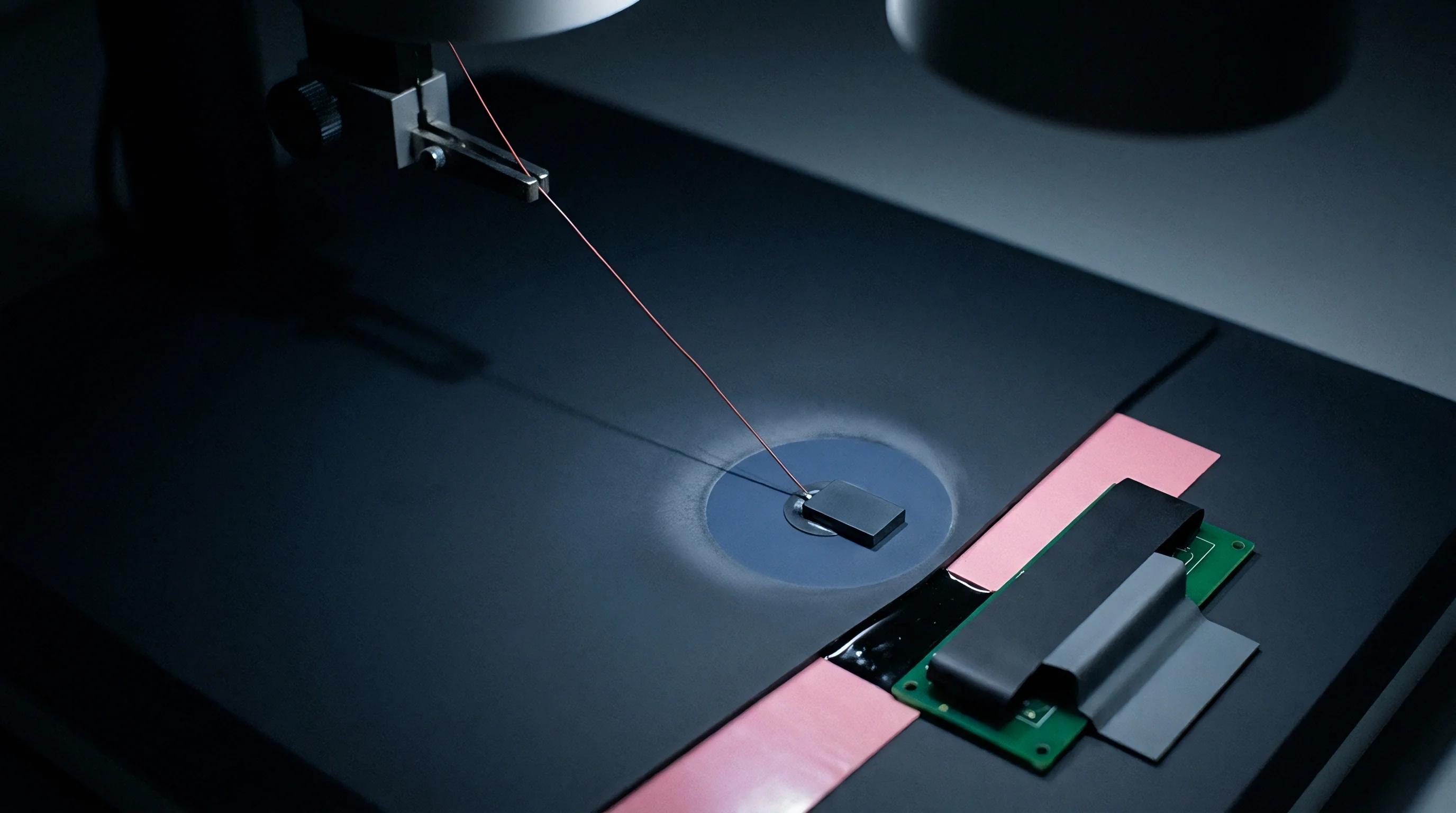
Package layouts often drop structural gaps into reference planes for mechanical, optical, or thermal reasons. Image sensor carriers use large rectangular cavity cutouts under or around the die for light access or silicon stress relief, while MEMS pressure and acoustic sensors require port openings straight through the substrate. These apertures force traces across reference plane edges, creating localized impedance steps and asymmetry between the positive and negative signal legs that degrade signal integrity before reaching the main board.
Ground Plane Cutouts and Cavity Window Effects
Optical sensor packages need open apertures over the active pixel array, forcing metal shielding layers to stop short near the die edge. High-speed output traces ~ like multi-lane MIPI CSI-2 lines ~ routing from die pads across the substrate to package pins inevitably cross this boundary between open cavity and solid plane. At the transition, odd-mode impedance spikes because capacitive coupling to ground drops away while mutual inductance between the traces stays the same.
Unshielded substrate spans inside cavity packages expose differential pairs to external noise and increase radiation loss. A trace crossing an open cavity gap can see its impedance jump from a nominal one hundred ohms to over one hundred fifty ohms across just a few hundred micrometers. That sudden change reflects high-frequency energy back toward the transmitter, creating standing waves that distort edge timing and close the data eye at the receiver PHY.
Trace pairs crossing an unshielded cavity window gap experience localized impedance jumps from one hundred ohms to over one hundred fifty ohms.
Fiber Weave Skew in Substrate Laminates
Woven glass fabric inside organic substrates creates localized dielectric gradients across closely spaced differential lines. Standard laminates like FR-4 and bismaleimide-triazine (BT) resin feature glass yarn bundles embedded in an epoxy matrix. Glass bundles have a relative dielectric constant between six point zero and six point five, while the surrounding epoxy runs lower, between two point eight and three point two.
If one line of a pair sits over a glass bundle and the other over a resin gap, each line sees a different effective permittivity.
Phase velocity varies inversely with the square root of the effective dielectric constant, so running a differential pair across a dielectric gradient creates propagation delay imbalance. Over a ten-millimeter trace, a dielectric mismatch of zero point five produces several picoseconds of skew between positive and negative paths. At multi-gigabit rates, even two picoseconds of phase skew converts notable differential energy into common-mode noise, cutting into receiver timing margins.
- Reference plane cross-overs force high-frequency return currents to travel along elongated perimeter paths, increasing loop inductance and generating radiative emissions.
- Fiber weave orientation alignment aligns traces parallel to glass bundle weaves, maximizing localized velocity skew across closely spaced differential paths.
- Differential anti-pad overlap merges via clearance holes into a single continuous void, reducing differential capacitance while preserving ground return plane symmetry.
- Substrate cavity step-downs disrupt trace-to-plane height consistency, creating impedance discontinuities at the physical transition boundary.
Aligning trace pairs symmetrically relative to substrate glass bundles prevents velocity mismatches without requiring board redesigns.


Conversion
Asymmetric attenuation between differential lines turns pure differential signals into common-mode voltage fluctuations. In an ideal setup, two lines carry equal voltages of opposite polarity, keeping net common-mode voltage at zero. When physical discontinuities inside a package affect one trace more than the other, amplitude or timing symmetry breaks down.
Mode conversion measures this imbalance ~ specifically how much differential energy converts to common-mode energy (Scd21) or reflects back as common-mode noise (Scd11).
Common-mode noise generated in sensor packages creates real performance risks. High-sensitivity systems ~ like millimeter-wave radar front-ends or low-noise optical image sensors ~ place quiet analog front-ends right beside high-speed digital output buses. Common-mode fluctuations corrupt ground planes, radiate EMI that risks regulatory compliance, and couple into sensitive analog nodes.
Stopping mode conversion requires tight geometric symmetry across every element in the package.

What Drives High-Frequency Phase Skew in Package Transitions?
Length differences between positive and negative conductors cause unequal propagation delays at gigahertz speeds. In compact packages, routing pairs around die corners, vias, or pad escapes often forces one trace into a slightly longer path. A mismatch of just fifty micrometers in an organic substrate generates tens of femtoseconds to picoseconds of phase skew, preventing signals from crossing at fifty percent of their peak-to-peak amplitude.
Unbalanced parasitic loading along the signal path also drives phase skew. If a structural via or power plane flood sits closer to one trace than the other, capacitive loading becomes uneven. The trace with higher capacitance shows a slower rise time, distorting the differential waveform, shifting the crossover point off baseline, and generating common-mode noise pulses on every transition.

Common-Mode Noise Generation and EMI Radiations
Unbalanced differential signals generate high-frequency electromagnetic emissions that couple directly into adjacent low-noise analog amplification stages. The common-mode voltage waveform (Vcm) produced by asymmetrical trace discontinuities is calculated as one-half the sum of the positive and negative line voltages:
Vcm = fracVp + Vn2
In a balanced system, Vp = -Vn and Vcm = 0. When phase skew (Δ t) or amplitude imbalance (Δ A) is present, Vcm oscillates at clock harmonics, driving high-frequency currents through ground planes and cable shields and turning package traces into small dipole antennas.
Four-port mixed-mode S-parameters quantify mode conversion severity, where Scd21 defines the ratio of output common-mode voltage to input differential voltage. Standard MIPI CSI-2 and PCIe specifications cap Scd21 below minus twenty decibels across the fundamental data band. Exceeding that threshold increases receiver bit-error rates (BER) and leads to failures during EMC qualification.
Excessive common-mode conversion degrades receiver jitter tolerance, causing intermittent link drops during high-throughput burst transmissions.


Topography
Layer stackup design determines the electromagnetic environment for differential traces from die pads down to PCB solder spheres. Engineers balance trace cross-sections, dielectric thicknesses, and copper plane layouts to hold uniform transmission line properties. Organic substrates use high-density interconnect (HDI) stackups with build-up micro-vias, thin dielectric films, and trace widths down to fifteen micrometers.
Keeping topography consistent across multi-layer transitions avoids unexpected impedance drops and phase distortion.
Substrate routing relies primarily on microstrip and stripline configurations. Microstrip traces sit on outer layers, making escape routing from die pads straightforward, though it leaves conductors exposed to dielectric variations in solder mask and air. Striplines run on internal layers between dual reference planes, offering better shielding and controlled impedance.
Switching between microstrip and stripline layers through micro-vias introduces topographic discontinuities that require tailored compensation structures to preserve signal integrity.

Substrate Layer Stackup and Redistribution Routing
High-density interconnect substrates use sequential build-up dielectric layers to route multi-gigabit signals through tight via pitches. Wafer-level designs rely on thin redistribution layers (RDL) made of polyimide or benzocyclobutene (BCB) deposited directly on the wafer. RDL trace widths and spacings run from two to ten micrometers, allowing fine-pitch escapes from dense die arrays.
However, thin dielectric layers (typically three to seven micrometers) place reference planes close to traces, forcing narrow trace widths to meet eighty-ohm or one-hundred-ohm target impedances.
Outer microstrip traces need protective solder mask coatings. Solder mask materials carry high dielectric loss tangents (typically zero point zero two to zero point zero three at five gigahertz) and vary in thickness over copper. Shifts in solder mask thickness between fifteen and thirty micrometers alter the effective dielectric constant (varεeff), changing trace impedance by up to eight percent.
Internal stripline routing avoids solder mask variations entirely by enclosing traces in uniform, low-loss dielectrics like glass-reinforced BT resin or organic laminates.
| Layout Mechanism | Structural Modification | Impedance Impact (Zodd) | Common-Mode Suppression (Scd21) | Manufacturing Complexity |
|---|---|---|---|---|
| Via Anti-Pad Enlargement | Merged Oval Clearance Void | Increases Zodd by +8 Ω to +15 Ω | Improves Scd21 by -4 dB to -7 dB | Low (Standard Drill/Etch) |
| Differential Pair Neck-Down | Trace Width Reduction at Pad Entry | Prevents Zodd dip (-10 Ω restored) | Improves Scd21 by -3 dB to -5 dB | Medium (Tight Etch Tolerance) |
| Ground Guard Trace Insertion | Coplanar Ground Shield Traces | Stabilizes Zodd within ± 2 Ω | Improves Scd21 by -8 dB to -12 dB | High (Consumes Substrate Space) |
| Asymmetric Pad Compensation | Staggered Tuning Stub Addition | Cancels localized Cpad spikes | Improves Scd21 by -5 dB to -9 dB | High (Precision EM Simulation) |

Compensation Structures and Anti-Pad Optimization
Recessing reference plane cutouts under landing pads mitigates capacitive load spikes. When a substrate via or land pad passes through a ground plane, the opening formed in the copper is an anti-pad. Standard round anti-pads create separate clearance holes for a differential via pair, leaving a narrow strip of copper between them.
That copper strip adds parasitic capacitance between each via barrel and ground, dropping local differential impedance.
Merging the clearances into a single oval anti-pad removes that copper strip between the vias. This continuous window lowers via-to-ground capacitance while keeping mutual inductive coupling between the via barrels intact, holding odd-mode impedance near one hundred ohms. Adding teardrop transitions at pad entry points also prevents sharp cross-sectional steps, smoothing electric field profiles and lowering high-frequency reflections.
Applying merged oval anti-pads around differential package vias eliminates localized capacitive impedance drops of up to fifteen ohms.
- Establish substrate layer stackup boundaries by selecting uniform dielectric layer thicknesses and copper foil weights that match target transmission line geometry.
- Apply symmetric differential escape routing from die bonding pads to ensure equal line lengths and trace environments during layer transitions.
- Optimize anti-pad clearances around all package micro-vias and landing pads using four-port electromagnetic field solvers to balance parasitic L and C.
- Incorporate coplanar ground shielding traces adjacent to high-speed differential pairs when routing across open cavity regions or outer package layers.
- Enforce tight manufacturing tolerance notes on master package drawings, specifying maximum trace etch variations within plus or minus ten percent.
Specifying IPC-2221 Class 3 trace etch tolerances of plus or minus ten percent on substrate production drawings prevents uncompensated impedance shifts across high-volume manufacturing lots.


Bench
High-bandwidth time-domain reflectometry pinpoints differential impedance spikes within packaged sensor assemblies. Discontinuities across sensor substrates occur over sub-millimeter distances, requiring high-resolution bench testing to separate die pad capacitance from substrate via stubs and landing ball mismatches. Signal integrity verification combines time-domain and frequency-domain measurements to evaluate package hardware against specifications.
Time-Domain Reflectometry (TDR) injects fast voltage steps ~ with rise times under fifteen picoseconds ~ into the package while tracking reflected amplitude over time. Reflection delays map directly to physical distance along the signal path using the dielectric’s propagation velocity. Plotting impedance (Z(t)) against position allows engineers to locate capacitance dips at landing pads or inductive spikes at wire bonds down to hundred-micrometer resolution.

High-Frequency S-Parameter Characterization
Vector network analyzers evaluate four-port differential insertion and return loss up to forty gigahertz. Testing relies on a calibrated Vector Network Analyzer (VNA) connected through micro-coaxial wafer probes. Mixed-mode S-parameters record differential behavior (Sdd11, Sdd21), common-mode behavior (Scc11, Scc21), and mode conversion (Scd11, Scd21).
Differential return loss (Sdd11) tracks reflected energy from impedance discontinuities along the path. Target specifications typically require Sdd11 better than minus fifteen decibels up to the fundamental clock frequency and better than minus ten decibels at the second harmonic. Differential insertion loss (Sdd21) measures total attenuation through the package; sharp drops or unexpected notches in Sdd21 point to stub reflections or cavity coupling that degrade data transmission.

Worked Impedance Mismatch Reflection Model
Evaluating a ten gigabit per second optical sensor interface operating over an eighty-ohm differential line illustrates the impact of a short substrate discontinuity. Consider a CMOS image sensor package with a zero point eight millimeter substrate trace section where pad capacitance drops differential impedance (ZL) to sixty-eight ohms, against an eighty-ohm nominal source and load (Z0). The signal has a 10 ~ 90% rise time (tr) of thirty-five picoseconds.
The voltage reflection coefficient (Γ) at the entrance boundary of the localized low-impedance discontinuity is calculated directly using the transmission line reflection equation:
Γ = fracZL – Z0ZL + Z0
Substituting the specific impedance values into the formulation yields:
Γ = frac68 – 8068 + 80 = frac-12148 ≈ -0.0811
This discontinuity reflects roughly eight point one percent of the incident differential voltage back toward the transmitter as a negative echo. The round-trip propagation delay (τ) through the zero point eight millimeter segment in organic BT dielectric (varεr ≈ 3.6) calculates using the speed of light (c ≈ 3 × 10⁸ m/s):
vp = fraccsqrtvarεr = frac3 × 108sqrt3.6 ≈ 1.58 × 10⁸ m/s = 0.158 mm/ps
τ = frac2 × 0.8 mm0.158 mm/ps ≈ 10.13 ps
Because round-trip delay (10.13 ps) is much shorter than the signal rise time (35 ps), the discontinuity behaves as a capacitive lump rather than a resolved transmission line. The peak reflected voltage step (Δ Vref) scales with rise time slope, distorting edge timing and adding peak-to-peak deterministic jitter (Δ tj ≈ 2.4 ps) to the data eye. Receiver equalizers must expend dynamic range to clear this reflection, reducing eye height margin at the host PHY detector.
Substrate trace discontinuities with round-trip propagation delays shorter than signal rise times act as capacitive lumps, degrading eye height margins at the receiver PHY.
- Time-domain reflectometry resolution checks require sub-fifteen-picosecond pulse generators to isolate individual micro-via impedance dips within compact package substrates.
- Mixed-mode S-parameter audits track differential insertion loss notches across forty-gigahertz spans to detect internal package cavity resonances.
- Receiver CTLE tuning steps adjust firmware equalizer gain boost parameters to compensate for measured package trace high-frequency attenuation roll-off.
- Micro-probing calibration procedures perform short-open-load-thru standards calibration at probe tips to eliminate test fixture parasitics from package measurements.
Whether silicon receiver equalization can entirely compensate for severe mode conversion caused by package cavity discontinuities without increasing die thermal dissipation remains an open question for ultra-compact sensor designs.


Procurement
High-speed sensor die reach production in multiple package variants that determine the final bill of materials. Vendors often build a single silicon sensor die ~ such as an image sensor or radar front-end IC ~ and offer it in three to five package configurations. Sourcing decisions evaluate how each option impacts board area, layer counts, high-speed routing risk, assembly yield, and unit cost.
Total landed cost extends well past component piece price. A bare chip-scale package keeps part cost down but shifts interconnect density onto the PCB, requiring expensive HDI micro-via stackups. Selecting an integrated module simplifies assembly and protects signal integrity, but multiplies piece price by three to five times.
Balancing these trade-offs requires weighing production volume, target yield, and bring-up schedules.

Package Form Factor Pricing Ladders
While silicon die cost stays constant, carrier structures change unit pricing by a factor of three or four. Wafer-Level Chip Scale Packages (WLCSP) offer the lowest initial piece price. However, mounting fragile WLCSP parts directly to the board demands tight reflow profiles, precise placement, and specialized underfill to prevent thermal-cycling fatigue in solder joints.
Standard QFN and substrate LGA options land in the middle tier, giving reliable mechanical protection and standard SMT handling at the cost of higher parasitic discontinuity risks. Flip-Chip Ball Grid Array (FCBGA) versions cost considerably more due to complex organic substrates, fine-pitch micro-bumps, and heat spreaders. Integrators move to FCBGA packaging when high-frequency signal integrity and strict mode conversion limits outweigh component piece price.
| Package Variant | Unit Price (50k volume) | Minimum Order Quantity (MOQ) | Board Assembly Yield | High-Speed Discontinuity Risk | Bring-Up Overhead (Weeks) |
|---|---|---|---|---|---|
| Wafer-Level CSP (WLCSP) | $4.20 per unit | 25,000 units (Tape/Reel) | 98.2% (Demands HDI PCB) | Low (Direct RDL Escapes) | 3 to 4 Weeks |
| Wire-Bonded LGA (64-pin) | $5.10 per unit | 10,000 units (Tray/Reel) | 99.6% (Standard SMT) | High (Bond Wire Inductance) | 5 to 7 Weeks |
| Flip-Chip BGA (121-ball) | $6.85 per unit | 5,000 units (Tray) | 99.4% (Standard SMT) | Low (Optimized Substrate) | 2 to 3 Weeks |
| Integrated Sensor Module | $14.50 per unit | 1,000 units (Box) | 99.9% (Drop-In Header) | Zero (Pre-Tested Bus) | 1 Week |

Sourcing Risk and Assembly Yield Trade-Offs
Selecting ultra-fine pitch wafer-level packaging shrinks board footprint but increases assembly defect rates. Ball pitches of zero point four millimeters or smaller yield lower SMT pass rates than standard zero point eight millimeter BGAs. Solder bridges, voids, and open traces on high-speed pin pads require X-ray inspection and manual rework, eroding initial packaging savings.
Minimum order quantities (MOQ) and lead times also diverge across package types. Standard LGA and QFN sensors are stocked through distribution channels with lead times of four to eight weeks. Specialized FCBGA or module variants need factory-direct runs with lead times over twenty-four weeks and MOQs exceeding ten thousand units.
Procurement teams must account for these logistics before locking schematic land patterns and carrier choices.
Evaluating the total landed cost of high-speed sensor integration requires balancing initial package piece price against printed circuit board layer stackup cost, substrate yielding loss, and driver bring-up duration.