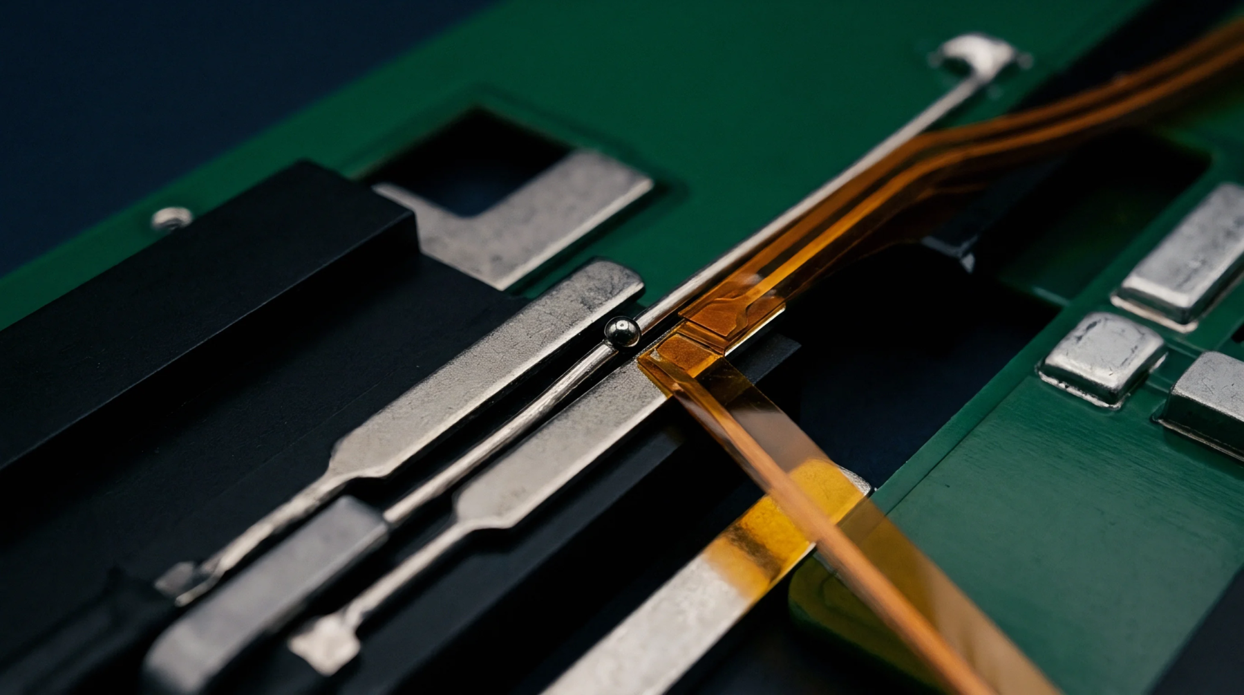
Assembly Method
Solder joints hold electrical components directly against the copper pads on the exterior of a printed circuit board. Surface mount technology facilitates high density component placement by eliminating the need for through-hole leads that pass entirely through the substrate. This configuration reduces the overall physical footprint of the assembly while shortening signal paths for high frequency operations.
Thermal Resistance
Heat dissipation performance depends upon the thermal conductivity of the solder material and the contact area between the device and the board. Surface mount packaging designs influence the junction temperature of semiconductors during heavy load periods. Engineers measure this resistance from the active silicon die to the board surface to quantify the cooling efficiency of a specific layout.
Alignment Precision
Automated placement machines rely upon vision systems to detect component geometries before dropping them onto predefined solder paste deposits. Precise fiducial marks on the substrate ensure the equipment maintains sub-millimeter registration accuracy during the assembly cycle. Deviations from these marks cause bridges between adjacent pads or poor wetting that compromises the electrical continuity of the circuit.
Inspection Protocol
Automated optical inspection verifies the solder fillet geometry and the orientation of components after the reflow process completes. X-ray imaging provides a window into hidden joints underneath packages such as ball grid arrays where visual access remains blocked. These non-destructive testing methods confirm that the manufacturing output aligns with established quality standards for mechanical stability and electrical impedance.