
Piezoresistive Die Calibration Drift Mitigations for Wafer Level Assemblies
Wafer level piezoresistive die calibration drift settles through stress-decoupling bumps, thermal annealing schedules, and digital polynomial register trims.
Wafer level piezoresistive die calibration drift settles through stress-decoupling bumps, thermal annealing schedules, and digital polynomial register trims.
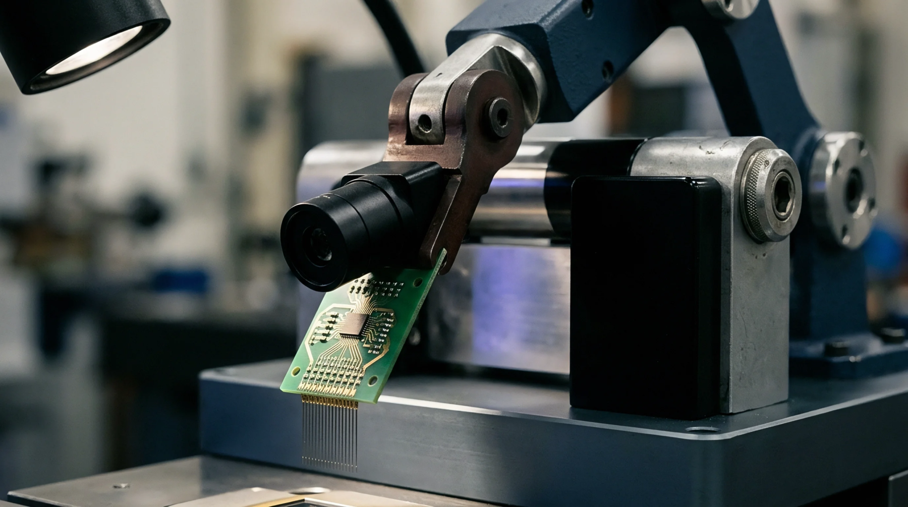
Fine-pitch solder joints under cyclic thermal stress require standoff height optimization and Anand model viscoplastic strain partitioning to prevent premature shear failure.

Fine-pitch WLCSP stencil apertures require area ratios above 0.66, using electroformed foils and rounded square designs to secure clean paste release.
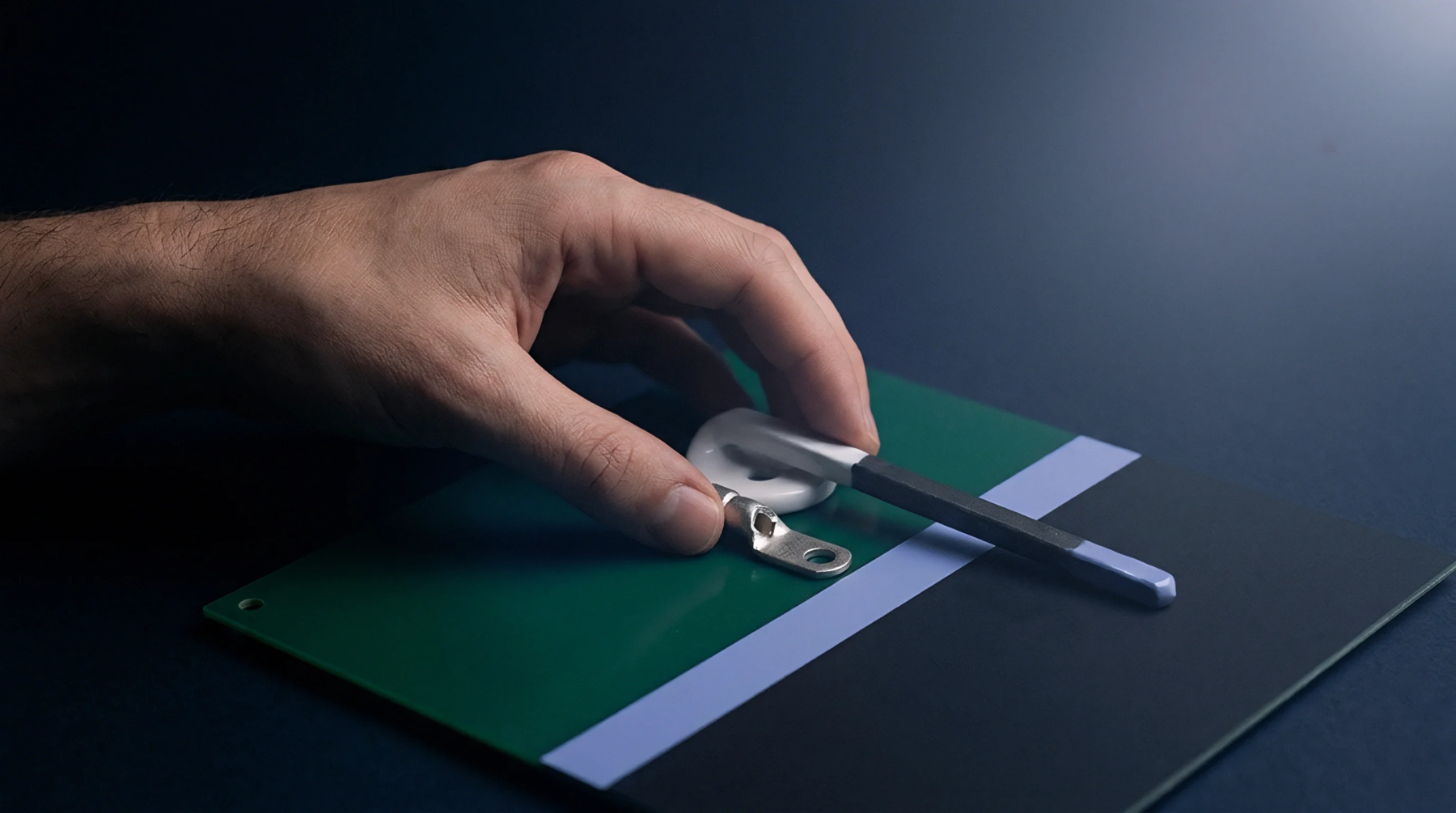
Plastic Quad Flat Package terminal breakout inductance stems from leadframe length and return loop area, requiring tight decoupling and ground plane continuity.

Tuning high-speed differential land patterns with plane cutouts and stencil reductions restores target impedance and preserves signal eye opening.
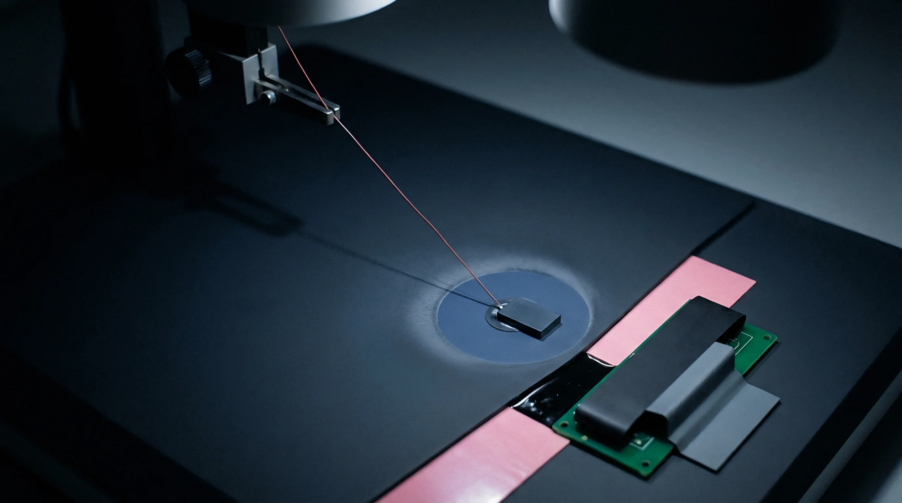
Co-optimizing substrate buildup layer microvias with board antipad geometry recovers 9 dB return loss at 28 GHz and relaxes PCB fabrication tolerances.

Solder fatigue life in large bottom-terminated components depends on maintaining a fifty-micrometer standoff to dissipate thermal shear energy.

Modifying leadless land pattern toe extensions and controlling stencil apertures increases solder standoff height, mitigating thermal fatigue failure in automotive modules.

Calculating solder expansion mismatch requires multiplying CTE differential, temperature delta, and distance to neutral point to determine thermal joint strain.

Asymmetric microvia lands in nitrogen reflow induce capillary solder wicking, tilting surface-mount ICs unless aperture compensation or VIPPO plating is specified.

Calculating tolerance stacks for ultra fine pitch footprints prevents solder bridging and open circuits by allocating variations across board etch and placement.
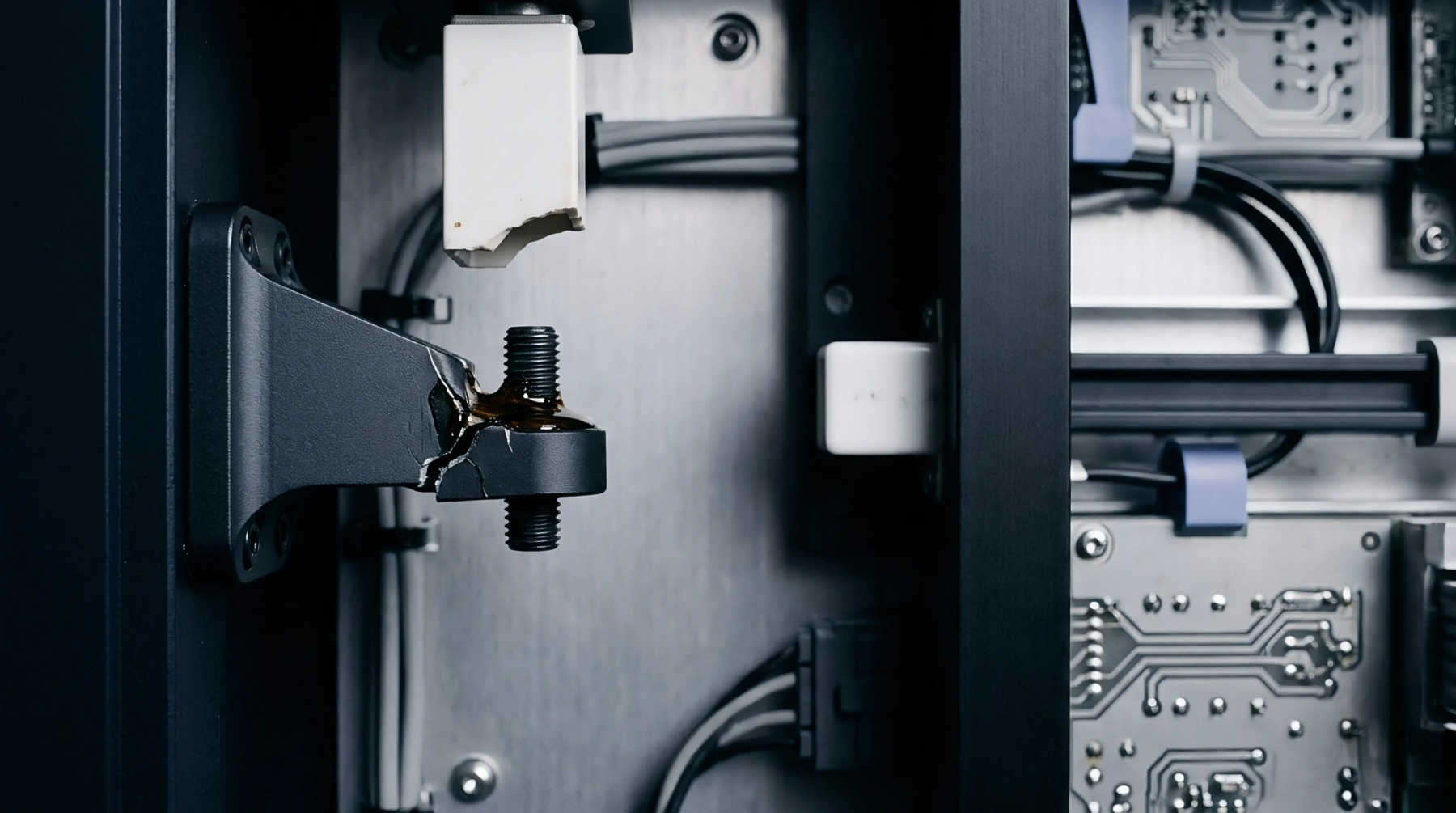
Micro-etched leadframes prevent package delamination during 260°C reflow by raising Mode I fracture toughness to bulk resin cohesive limits.

Hydrothermal aging degrades copper-polymer cohesive strength, requiring inverse FEA parameter extraction to prevent solder shock delamination.

Delamination in molded power IC packages stems from combined normal and shear interfacial stresses during reflow, mitigated by micro-etched leadframes and low-moisture resins.
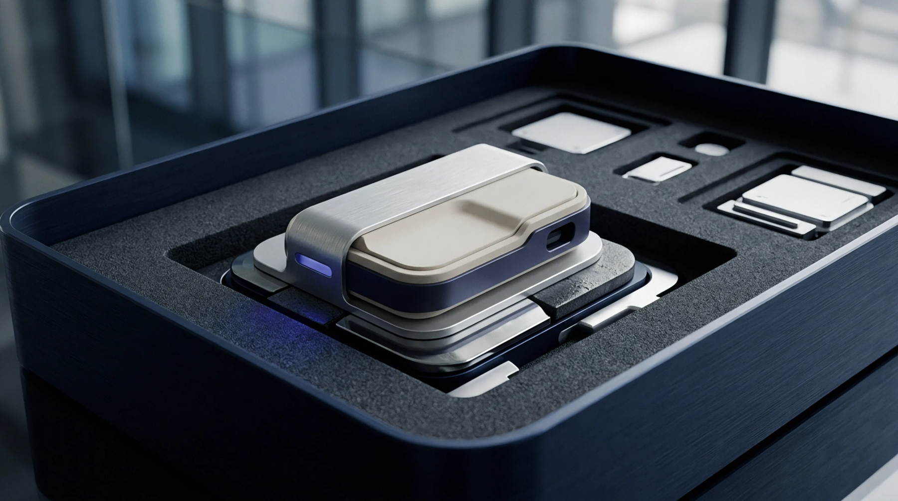
Multi-cycle baking accelerates Kirkendall void growth across nickel barriers, degrading shear strength and driving register offset drift on package pads.

A minimum 2.54 micrometer sulfamate or amorphous electroless nickel underplate prevents copper outdiffusion and solderability loss during extended bakes.

Terminal baking converts Cu6Sn5 to Cu3Sn via parabolic solid-state diffusion, driving Kirkendall voiding and sensor strain shift unless nickel barrier plating limits compound growth.

Accurate reflow delamination modeling requires coupling temperature-dependent cohesive zone parameters with 260°C hygrothermal vapor pressure calculations.
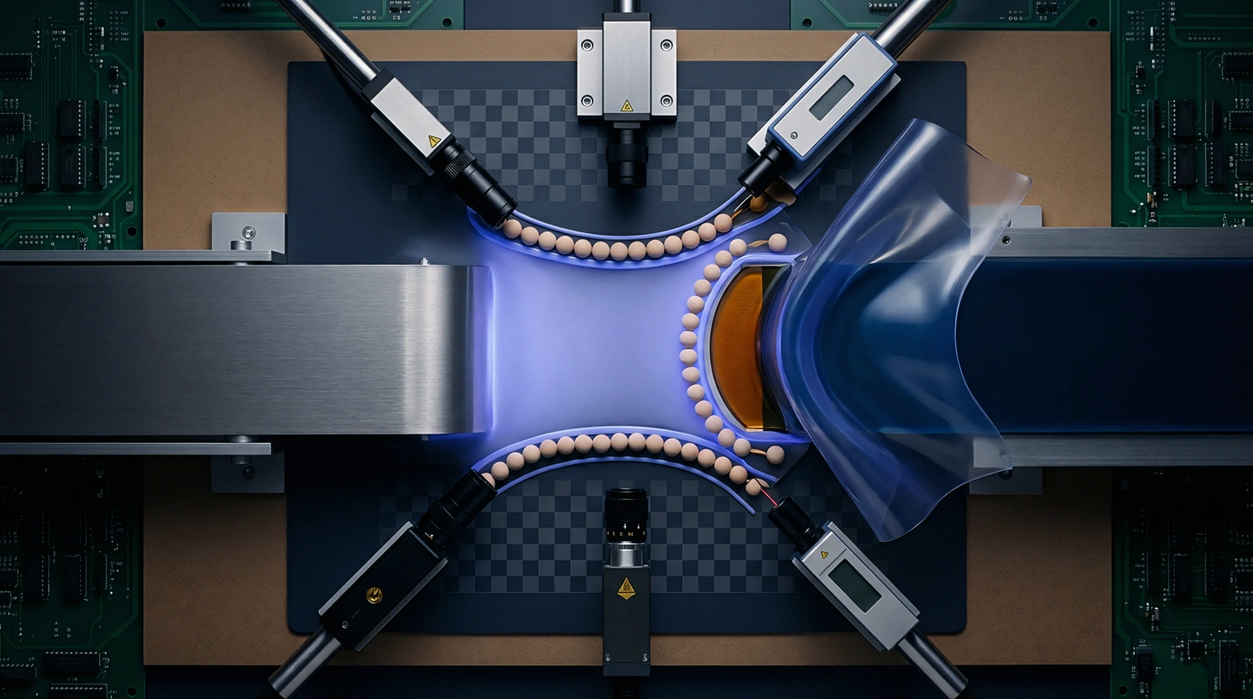
Non-equilibrium desorption kinetics dictate that rapid convection reflow vaporizes trapped micro-void moisture faster than diffusion can release it.
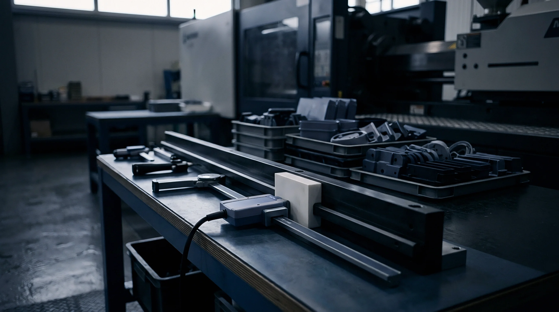
Transient hygrothermal diffusion modeling predicts mold compound swelling, prevents reflow popcorning, and eliminates sensor zero-point drift.

High silica molding compounds exhibit dual-stage non-Fickian moisture trapping that causes reflow vapor spikes and long-term strain offset drift.

Dynamic package warpage driven by moisture absorption and thermal expansion mismatch requires precise stencil volume compensation to prevent solder opens.

Leadless sensor floor life management requires derating MSL exposure hours and enforcing dry cabinet controls to prevent reflow delamination and calibration drift.

Non-Fickian dual-site kinetics models prevent package popcorning by accurately predicting vapor pressure spikes during rapid reflow ramps.

Extract desorption activation energy using multirate Kissinger plots to establish accurate package bake profiles and micro-cavity vacuum lifespan predictions.

Polymer moisture absorption kinetics determine plastic package floor life and determine thermal baking requirements before lead-free reflow assembly.

Symmetric land copper balancing and 35 percent stencil aperture segmentation suppress reflow tilt and piezoresistive offset drift in asymmetric BTC packages.
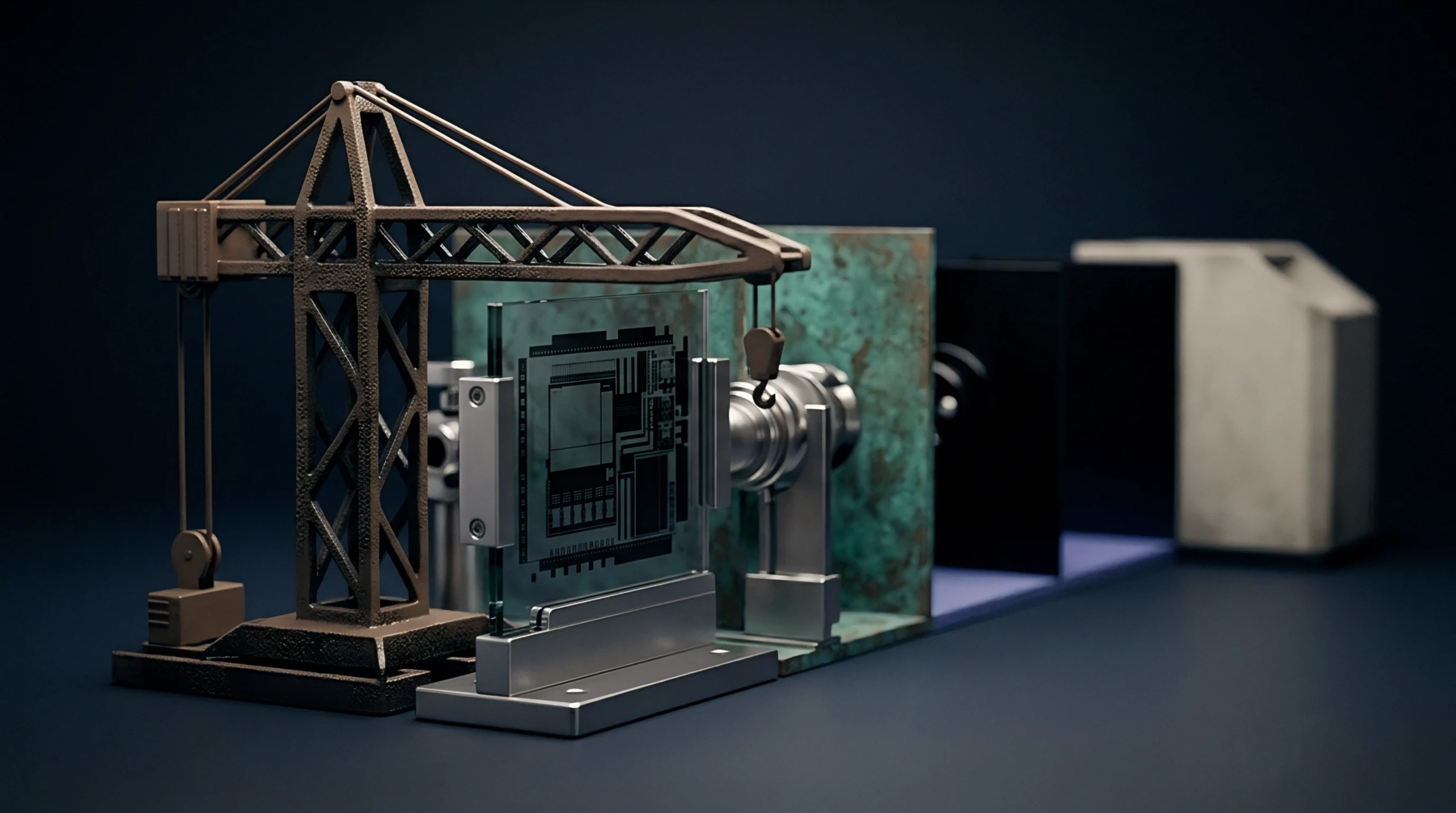
Reflow profiling for mixed MSL boards demands balancing maximum package body temperatures against solder liquidus duration to prevent internal delamination.

Receiving operators verify moisture barrier pouch vacuum integrity, heat seals, and indicator cards before resetting component exposure timers.
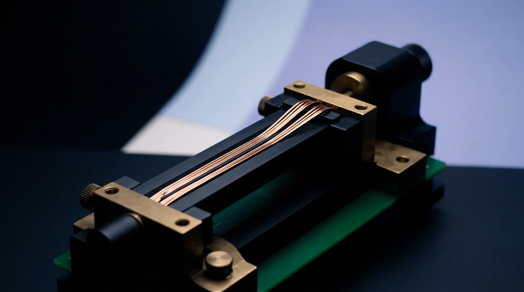
Resolving flexure-induced relaxation oscillator drift requires compliant silicon die attach adhesives, board strain relief routing, and host clock stretching support.
Expertise is a utility, not a secret. sentiention™ publishes its working knowledge as open reference: intelligence layer covering the materials it sources, the markets it enters, and the reference that serves both.