Stress Decoupling Buffer Selection for Piezoresistive Pressure Sensor Packaging
Stress decoupling buffers isolate piezoresistive pressure sensor dies from thermal expansion and board flexure, preserving baseline zero-offset calibration stability.

Isolation
Parasitic shear stress reaching the active Wheatstone bridge on a silicon membrane causes a zero-point offset shift in piezoresistive pressure sensor dies. Single-crystal silicon has a high piezoresistive coefficient, with longitudinal strain altering surface resistor values by up to sixty percent under full-scale pressure. When solder reflow cooling, substrate warpage, or housing forces flex the underlying carrier, these distortions pass directly into the diaphragm.
Single-crystal silicon carries a thermal expansion coefficient of 2.6 parts per million per Kelvin, while standard FR-4 circuit board material expands at 14 to 17 parts per million per Kelvin. Without structural attenuation, this thermal mismatch drives micro-strain into the silicon substrate, pushing the uncalibrated zero-scale output voltage past the correction limit of integrated signal conditioning circuits.

Mechanical Strain Pathing in Surface Mount Housing
Board assembly imposes heavy mechanical loads on surface-mount pressure sensor packages during reflow and final installation. Solder joint solidification between 217 and 260 degrees Celsius locks the leadframe or ceramic substrate into structural tension with the printed circuit board. As the assembly cools to ambient room temperature, differential contraction creates bending moments across the package base.
In molded plastic packages like Small Outline Integrated Circuit (SOIC) or Land Grid Array (LGA) footprints, the encapsulant transfers board flexure straight to the die edges. Mechanical stress travels from the solder pads through the leadframe or laminate substrate, across the die-attach adhesive, and into the active piezoresistors on the MEMS membrane surface.
Evaluating how well these parasitic forces are attenuated requires examining the shear modulus and thickness of each layer along the stress path. Thick, low-elasticity die-attach adhesives function as mechanical low-pass filters, absorbing high-frequency deformations from board twist or housing torque. If the die-attach layer is too thin or has a high shear modulus, packaging stress moves directly into the silicon substrate without dampening.
That transferred stress disrupts the symmetry of the piezoresistive bridge, producing a thermal offset drift that looks identical to a pressure change. Low-pressure sensors ~ specifically those below 100 kilopascals ~ are especially vulnerable to packaging strain because their membranes are often under fifteen micrometers thick.
Decoupling buffers must absorb board contraction stress before parasitic strain distorts the active sensing diaphragm.

Shear Stress Coupling across Die Attach Interface
Direct mechanical coupling between the silicon die and carrier substrate is the primary cause of unrepeatable zero-offset drift during thermal cycling. Standard epoxies in non-sensing packaging have high Young’s modulus values exceeding 3 gigapascals at room temperature. Placing these rigid adhesives directly beneath a piezoresistive pressure sensor die forces thermal contraction straight into the bulk silicon.
Ion-implanted or boron-diffused piezoresistors respond to this residual strain by shifting nominal resistance, pushing zero-point drift past three percent of full-scale span over a 100-degree thermal window.
Shear stress concentrated at the corners of a rectangular die creates localized gradients across the membrane, unbalancing the Wheatstone bridge layout. A die-attach layer designed for stress decoupling minimizes shear coupling by lowering its shear modulus without compromising die retention during physical shock. Keeping the adhesive modulus below 5 megapascals stops substrate warpage from reaching the bulk silicon.
Choosing an improper bonding material leads to permanent zero-point shifts after thermal shock testing, preventing the assembly from maintaining factory calibration over its operating life.

Elastomers
Silicone gels and low-modulus elastomers act as buffer layers, isolating the piezoresistive die from mechanical stress and aggressive media. With Young’s moduli often below 100 kilopascals, these soft polymers deform under packaging strain without transferring load to the silicon membrane. Applied as a potting compound over an exposed MEMS sensor, a soft gel transmits fluid pressure hydrostatically to the diaphragm while absorbing high-frequency vibration and assembly stress.
Gel chemistry ultimately sets the long-term drift profile under thermal swings and chemical exposure.

Viscoelastic Modulus Drift across Operating Temperature Ranges
Temperature swings alter the mechanical compliance of polymeric buffers and degrade their stress isolation. Silicone formulations enter glass transition anywhere between minus 40 and minus 120 degrees Celsius. As ambient temperatures approach glass transition, the gel’s Young’s modulus rises by several orders of magnitude, turning a soft, stress-absorbing material into a rigid solid.
This stiffening compromises buffer decoupling, allowing thermal contraction to couple directly into the piezoresistive die at low temperatures.
Thermal expansion of the gel adds another stress vector when confined inside a rigid package cavity. Silicone gels feature high volumetric expansion coefficients, typically between 800 and 1000 parts per million per Kelvin. If the package cavity lacks sufficient headspace, heating causes the gel to press directly against the sensor membrane and thin wire bonds.
This confinement stress alters span calibration and can shear gold or aluminum wire bonds from their pads. Designers specify tight fill volumes and headspaces above the gel to accommodate volumetric growth across the operating temperature range.
Silicone gel with a Young’s modulus below 50 kilopascals at room temperature hardens by three orders of magnitude below its glass transition temperature of minus 50 degrees Celsius.
| Buffer Material Type | Young’s Modulus (kPa) | Glass Transition Tg (°C) | Linear CTE (ppm/K) | Media Compatibility |
|---|---|---|---|---|
| Standard Dimethyl Silicone Gel | 15 to 45 | -120 to -110 | 300 to 350 | Dry air, non-corrosive gases |
| Fluorosilicone Gel | 35 to 85 | -65 to -55 | 280 to 320 | Fuel vapors, oils, solvent spray |
| Soft Epoxy Die Attach | 1500 to 5000 | -30 to -10 | 65 to 90 | High humidity, harsh chemicals |
| Polyurethane Potting Compound | 500 to 2000 | -45 to -35 | 180 to 240 | Water immersion, mild acids |
Media Compatibility and Vapor Penetration Constraints
Exposing standard dimethyl silicone gels to aggressive chemicals degrades the material and destroys decoupling performance. Automotive fuels, industrial solvents, and refrigerant oils diffuse into the siloxane matrix, swelling the gel and altering its mechanical properties. That swelling exerts localized pressure against the MEMS diaphragm, generating baseline drift indistinguishable from actual pressure changes.
Under severe exposure, solvent absorption breaks down the cross-linked gel network, stripping the buffer entirely from the cavity.
Fluorosilicone buffers incorporate trifluoropropyl groups along the polymer backbone to resist chemical attack and swelling. Electronegative fluorine atoms repel non-polar hydrocarbons, maintaining gel compliance in gasoline, diesel fuel, and engine lubricants. However, fluorosilicones carry higher room-temperature moduli and higher glass transition temperatures than pure dimethyl silicones.
While a fluorosilicone buffer blocks harsh media ingress, it restricts low-temperature operation due to material stiffening below minus 50 degrees Celsius.
Standard silicone gel formulations maintain stress decoupling in general industrial use, but solvent-induced swelling alters performance under chemical exposure. Field testing shows that unfluorinated gels swell by up to 25 percent by volume in automotive fuel vapors, destroying zero-point offset stability within fifty operational hours.

Pedestals
Intermediate glass or silicon submounts placed between the MEMS die and package carrier deliver strong stress isolation without relying entirely on polymeric adhesives. Borosilicate glass pedestals, such as Pyrex 7740, feature a thermal expansion coefficient of 3.25 parts per million per Kelvin, closely tracking silicon’s contraction across a wide temperature range. Placing a glass pedestal between the silicon sensing element and an alumina substrate or copper leadframe dissipates mechanical strain within the bulk glass before it reaches the diaphragm.
Pedestal height directly sets the attenuation ratio for board-level bending moments.
Submount Geometry and Glass Frit Bond Line Tolerances
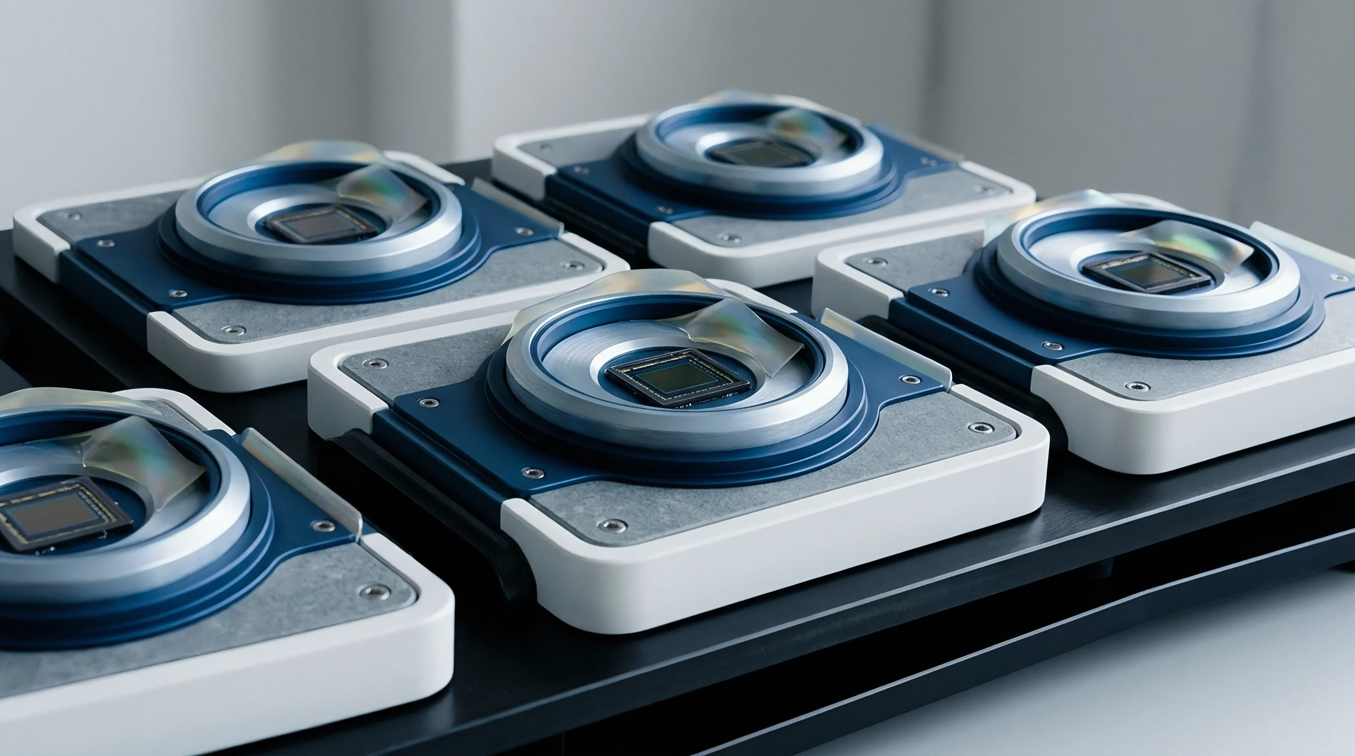
Pedestal aspect ratio controls mechanical isolation in surface-mount pressure sensor packages. Increasing the height-to-width ratio of a rectangular glass submount lengthens the stress path, dampening board warpage before it reaches the die interface. A tall, narrow pedestal isolates better than a flat, broad submount, but complicates automated placement and wire bonding.
High pick-and-place nozzle acceleration can shift tall pedestals before the bond line cures, causing tilt misalignment that degrades packaging tolerances.
Anodic bonding and glass frit bonding are the main techniques for securing the silicon MEMS die to a glass pedestal. Anodic bonding forms an atomic-level seal between polished silicon and borosilicate glass around 400 degrees Celsius under a high electrostatic field. This produces a hermetic, stress-free bond with zero voids, eliminating localized stress concentrations that distort the Wheatstone bridge.
Glass frit bonding screen-prints a low-melting glass paste onto the pedestal, curing it between 400 and 500 degrees Celsius. Though less costly than anodic bonding, frit layers require strict print-thickness control to prevent uneven thermal strain across the die base.
Standard JEDEC reflow specifications mandate that component packages survive thermal exposure up to 260 degrees Celsius without delamination of internal stress-decoupling bond lines.
- Die tilt misalignment exceeding 0.5 degrees creates asymmetric air gaps in gel-filled cavities, causing non-uniform hydrostatic pressure transfer across the MEMS diaphragm.
- Vibration resonance coupling occurs when the natural frequency of a tall pedestal assembly matches application vibration profiles, leading to bond line fatigue failure.
- Void formation in frit layers creates localized stress concentration points, causing unpredictable zero-offset shifts during thermal cycling.
- Interfacial delamination between the glass submount and organic substrates happens under heavy moisture exposure when vapor pressure builds up during solder reflow.
Thermal Expansion Matching with Silicon Sensing Elements
Matching thermal expansion coefficients across structural packaging layers minimizes residual stress introduced during high-temperature assembly. Mounting a silicon die directly to a copper leadframe ~ which carries an expansion coefficient of roughly 16.5 parts per million per Kelvin ~ creates heavy strain upon cooling from cure temperatures. A silicon pedestal eliminates thermal mismatch at the die interface entirely, shifting it down to the submount-substrate junction where stress is easier to manage.
Pedestals produced via deep reactive-ion etching yield tight dimensional tolerances and consistent geometry.
Submount materials must also withstand mechanical stresses imposed by thermal shock compliance protocols like AEC-Q100 Grade 0 testing. Rapid thermal swings between minus 50 and plus 150 degrees Celsius generate transient shear stresses at pedestal bond lines due to thermal lags across the package. Aluminum oxide and aluminum nitride ceramic submounts offer high thermal conductivity to reduce transient gradients, but present a larger thermal mismatch with silicon than borosilicate glass.
Operating requirements determine whether steady-state expansion matching or transient thermal dissipation dictates material selection.
Specifications for sensor packaging components frequently reference IPC-7093 standards for bottom-terminated components, setting maximum void ratios in submount adhesive layers to maintain stress isolation.

Conditioning
Application-Specific Integrated Circuits (ASICs) work alongside physical buffers to compensate for residual packaging stress through digital signal processing. Sensor signal conditioners integrate programmable gain amplifiers, analog-to-digital converters, and non-volatile memory storing thermal compensation coefficients. When mechanical stress flexes the piezoresistive die, the resulting shift in baseline resistance creates a zero-scale offset that the ASIC must trim.
While digital calibration removes predictable, repeatable shifts, it cannot correct non-linear stress hysteresis driven by viscoelastic gel creep or mechanical assembly movement.

EEPROM Trim Window Limits under Mechanical Package Distortion
Signal conditioning ASICs use polynomial equations to correct zero-point offset drift and temperature coefficients across the operating range. DAC channels dedicated to offset trimming have finite correction ranges, typically limited by 12-bit or 16-bit registers in internal EEPROM. If severe packaging strain shifts uncalibrated zero-offset voltage by more than 20 percent of raw bridge output, the required trim exhausts the available register window, leaving the ASIC unable to center output voltage within specification.
Using up too much of the calibration budget to offset mechanical package strain degrades overall signal resolution. Amplifying a heavily offset bridge signal requires high front-end gain, which simultaneously boosts baseline thermal noise and strain-induced non-linearity. Packages that fail to dampen substrate stress force calibration routines near their limits, lowering yields during production trimming.
Keeping raw bridge offsets tight through proper buffer selection preserves digital dynamic range to correct for real environmental temperature shifts.
Verifying bridge offset bounds during post-reflow bring-up requires executing a structured functional test sequence on standard production test fixtures:
- Apply nominal supply voltage to the sensor assembly while maintaining chamber temperature at 25 degrees Celsius in a zero-pressure environment.
- Measure raw unamplified Wheatstone bridge differential output voltage directly across the ASIC analog input pins using a high-impedance digital multimeter.
- Compare the observed zero-point voltage against raw die limits to confirm packaging stress has not shifted offset by more than 5 millivolts per volt of excitation.
- Take a second reading after soaking the assembly at maximum operating temperature for two hours to verify that buffer expansion has not driven bridge differential past the ASIC digital trim budget.
Can Digital Polynomial Compensation Overcome High Gel Stiffening?
Relying solely on digital compensation to correct for low-temperature gel stiffening fails because viscoelastic materials exhibit time-dependent mechanical hysteresis. Below glass transition, gel modulus changes become non-linear and sensitive to thermal ramp rates. A static polynomial in EEPROM cannot distinguish between steady-state cold exposure and rapid thermal shock, introducing uncorrectable hysteresis into the output stream.
Digital interfaces like I2C and SPI transmit compensated pressure values directly to host microcontrollers, hiding raw bridge behavior. When packaging strain turns non-linear, internal calibration algorithms calculate output based on stored coefficients that no longer reflect the stiffened gel’s physical state. The digital output streams smoothly, but reported pressure drifts from true line pressure ~ creating silent measurement errors that bypass basic firmware boundary checks.
| Interface Mode | Available Trim Range | Max Allowable Raw Offset | Calibration Resolution | Stress Sensitivity Risk |
|---|---|---|---|---|
| Ratiometric Analog (0.5V – 4.5V) | ± 15% of span | ± 8 mV/V | 12-bit DAC | High; amplifier saturation under heavy packaging tilt |
| I2C Digital Interface | ± 25% of span | ± 15 mV/V | 16-bit register | Medium; dynamic range compression under thermal stress |
| SPI Digital Interface | ± 25% of span | ± 15 mV/V | 16-bit register | Medium; register saturation at cold temperature extremes |
| SENT Protocol (SAE J2716) | ± 20% of span | ± 12 mV/V | 14-bit register | High; strict latency limits prevent iterative compensation |
Whether edge-processed calibration models will eventually enable unbuffered, high-stress plastic packages without glass pedestals remains an open question for automotive powertrain and radar monitoring units.

Procurement
Sourcing piezoresistive pressure sensors requires balancing unit package costs against firmware schedules and assembly yields. Bare MEMS dies represent a minor fraction of component cost, while stress-decoupling package features dictate final pricing. A bare die on a basic ceramic substrate carries a low unit price, but demands significant engineering effort to design, dispense, and calibrate stress buffers.
Fully potted, ASIC-conditioned SOIC-8 or LGA packages carry higher unit costs but eliminate raw bridge processing overhead.

Yield Degradation and Reflow Thermal Profiling Constraints
Automated high-speed assembly lines penalize delicate sensor packages through thermal profile mismatches and optical inspection failures. Decoupling buffers, especially soft silicone gels, restrict peak reflow temperatures and ramp rates. Exceeding J-STD-020 reflow limits causes gel outgassing, trapping air bubbles directly above the MEMS diaphragm.
These bubbles act as localized stress concentrators, degrading sensor accuracy and raising scrap rates during line testing.
Assembly yields drop quickly if automated dispensing strays from tight volume tolerances. Dispensing too much gel causes cavity overflow, solder pad contamination, and leadframe bridging. Too little gel leaves top-surface wire bonds exposed to moisture and vibration, inviting field failures.
Sourcing specifications should mandate automated vision tracking and post-cure weight verification to hold consistent yields across volume production runs.
- Verify gel viscosity specs on incoming certificates to prevent batch-to-batch variation in decoupling layer thickness.
- Audit supplier cleanroom standards to ensure zero particulate contamination enters open package cavities before buffer dispense.
- Require automated optical inspection data for gel fill height to guarantee consistent headspace across production lots.
- Validate reflow profile compatibility using dummy boards populated with thermocouple-instrumented packages prior to production release.
| Package Form Factor | Relative Unit Cost | Buffer Type Included | Integration Firmware Weeks | Target Application Class |
|---|---|---|---|---|
| Bare Die on Ceramic Submount | 1.0x | None (Requires user fill) | 8 to 12 weeks | High-volume automotive custom modules |
| Gel-Filled Plastic SOIC-8 | 2.8x | Dimethyl Silicone Gel | 2 to 4 weeks | Industrial process monitoring, HVAC systems |
| Hermetic Ceramic LGA | 5.5x | Fluorosilicone / Glass Frit | 1 to 2 weeks | Medical diagnostics, harsh media sensing |
| Stainless Steel Housed Module | 18.0x | Oil-Filled Isolator Diaphragm | 0 weeks (Analog/Modbus ready) | Heavy off-highway hydraulic lines |
Selecting a sensor package with an integrated decoupling buffer and factory-calibrated ASIC reduces integration risk, ensuring predictable landed costs in volume production.