Surface Mount Circuit Board Strain Measurement Best Practices
Verify ICT and depaneling strain rates below IPC/JEDEC-9704 dynamic limits using three-wire triaxial rosettes placed within two millimeters of package corners.
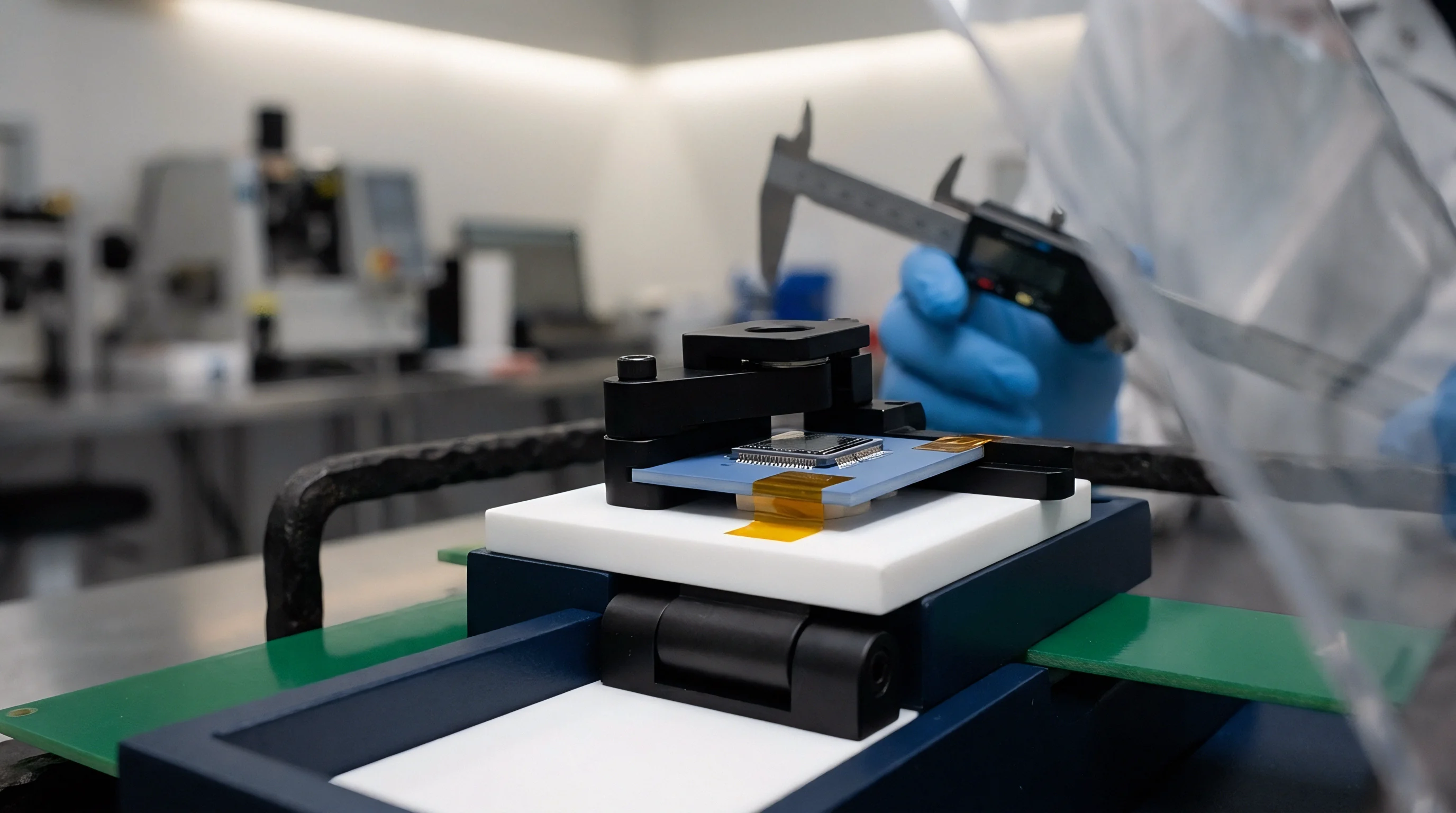
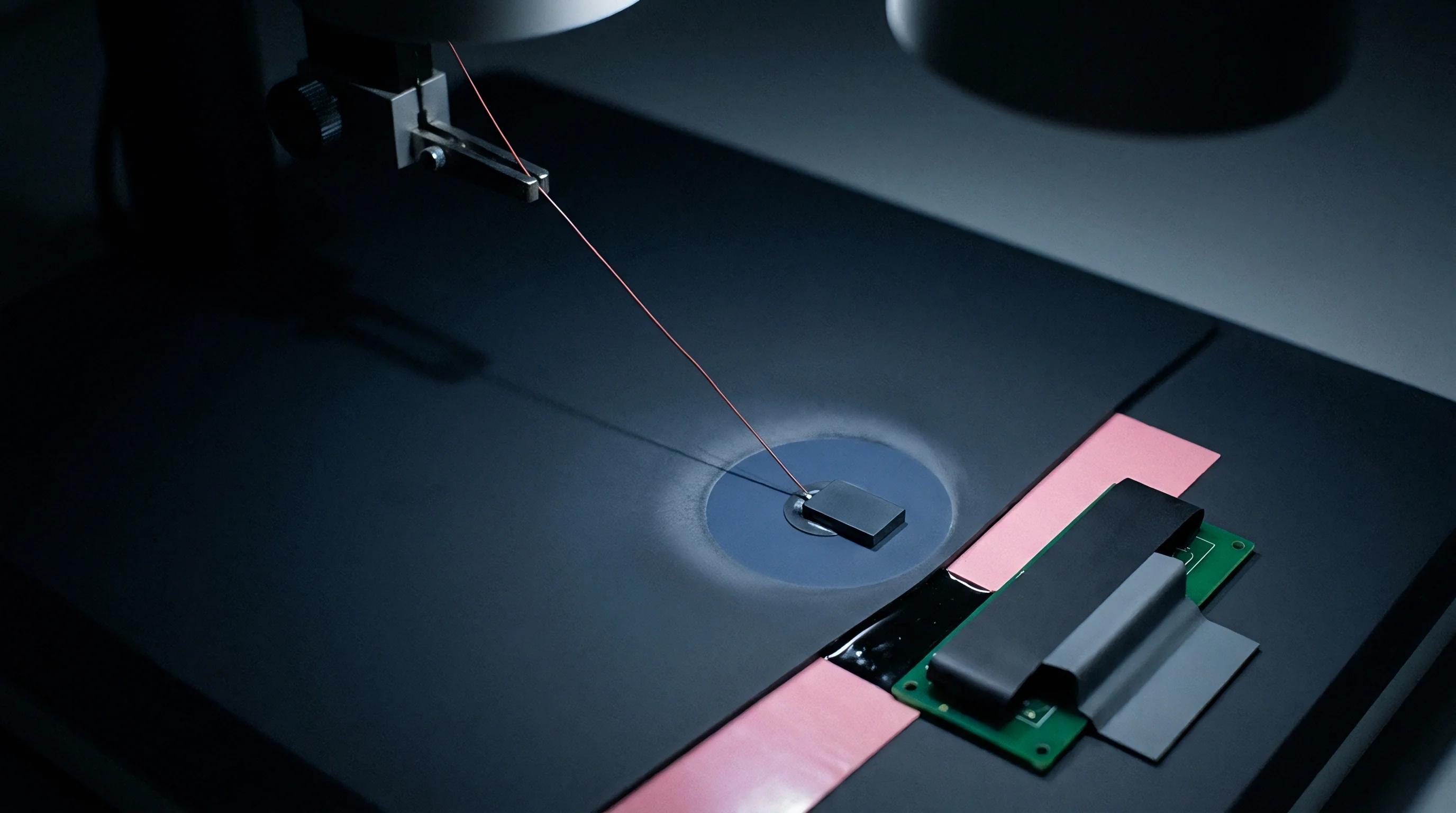
Foil
Substrate flexure during depaneling, connector insertion, and bed-of-nails testing can shear solder joints before a board ever sees a chassis. Foil strain gauges bonded directly to FR-4 translate this mechanical deflection into resistance shifts. Selecting the right element determines whether the recorded microstrain reflects actual copper pad displacement or just adhesive creep.
Constantan alloy on polyimide backing offers self-compensation matched to the 16 ppm per degree Celsius expansion coefficient typical of glass-reinforced epoxy. For thermal cycles above 200 degrees Celsius, Karma alloy variants are used, though their extra stiffness and cost make them trickier to bond in tight spaces.
Grid resistance generally comes down to 120 ohms or 350 ohms. The 350-ohm option cuts thermal dissipation across the bridge by roughly two-thirds at the same excitation voltage, preventing localized laminate heating that would otherwise cause baseline drift during long logging runs. When measuring near fine-pitch BGAs and QFNs, compact grids are essential.
Active lengths run from 0.38 millimeters up to 2.0 millimeters; smaller grids catch localized strain peaks at component corners, while larger ones average displacement across a wider area and can hide peak values.
Constantan gauges matched to sixteen parts per million per degree Celsius eliminate thermal offset error when ambient test temperatures stay within five degrees of baseline.
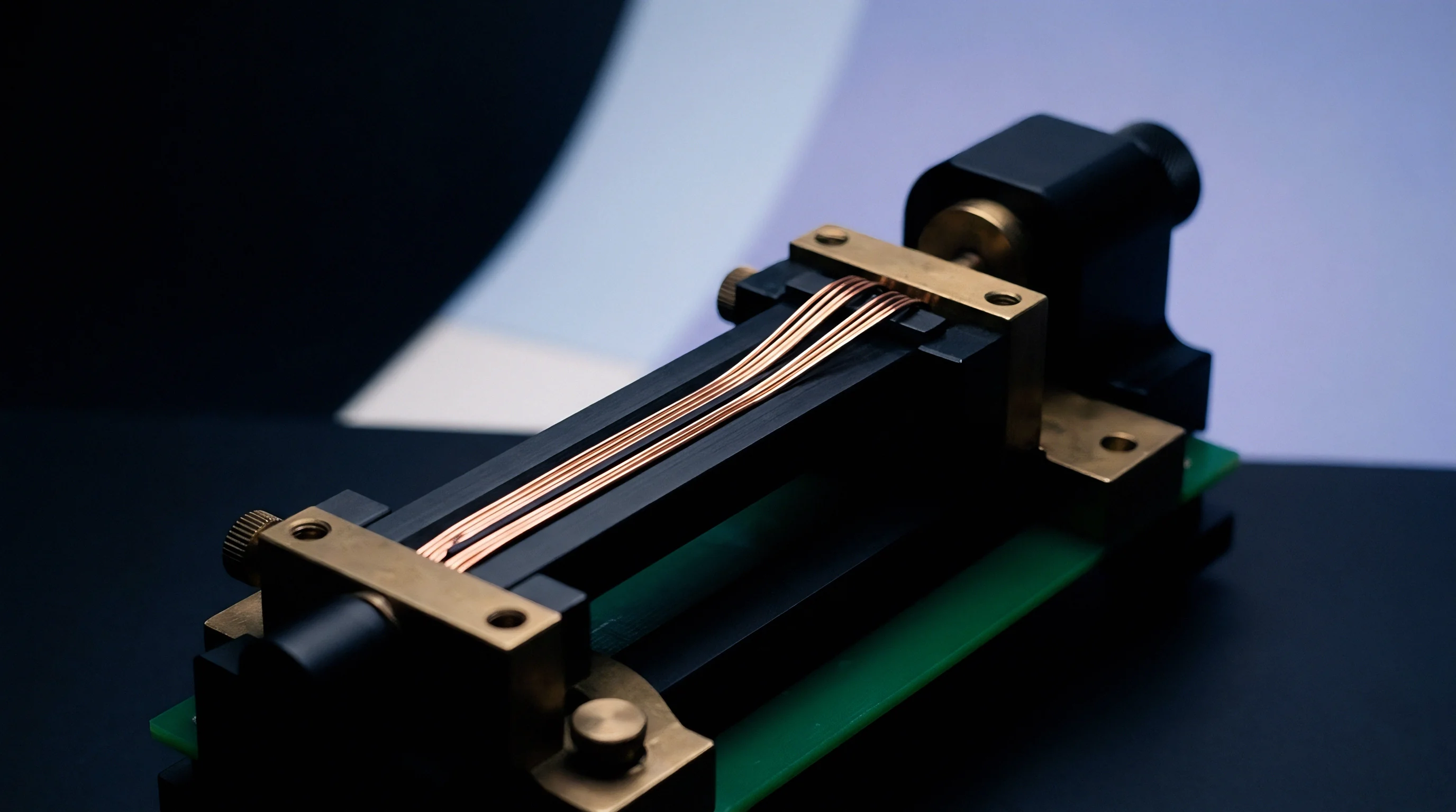
Gauge configuration depends on how complex the local stress field is. Where the principal strain axis does not align cleanly with board edges, biaxial or triaxial rosettes are needed to resolve multi-directional vectors. Stacked rosettes layer three foil grids into one footprint, keeping the sensing center compact but adding thickness and increasing shear attenuation through the glue.
Planar rosettes place three grids side-by-side on one polyimide backing, ensuring each grid sits directly on the substrate. The trade-off is a two-millimeter spread between sensing centers, which introduces spatial averaging errors across sharp strain gradients.
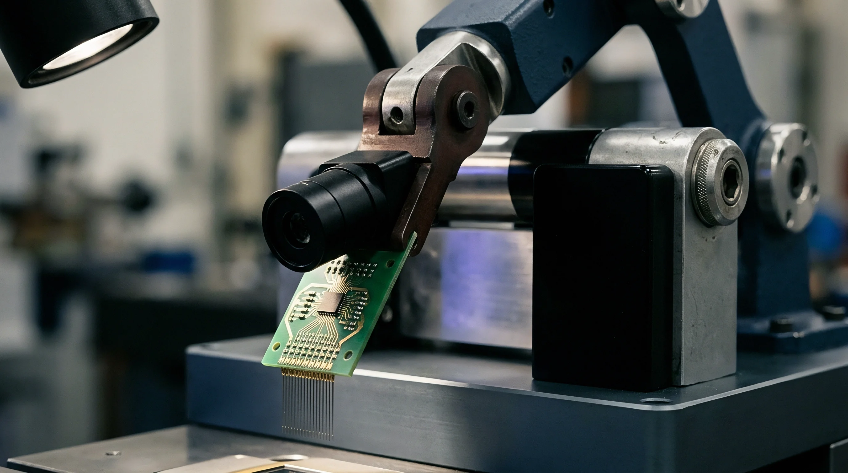
Pre-attached leads prevent heat damage to the polyimide carrier by eliminating soldering over active pads. Factory ribbon leads with fluoropolymer insulation keep a low profile, clearing nearby passives when test fixtures close. For fast ICT fixture checks, cyanoacrylates set within two minutes; for multi-day shock and vibration testing, clamp-cured modified epoxies provide much better fatigue resistance.
Thin glue lines transfer strain directly, avoiding elastomeric damping.

Placement
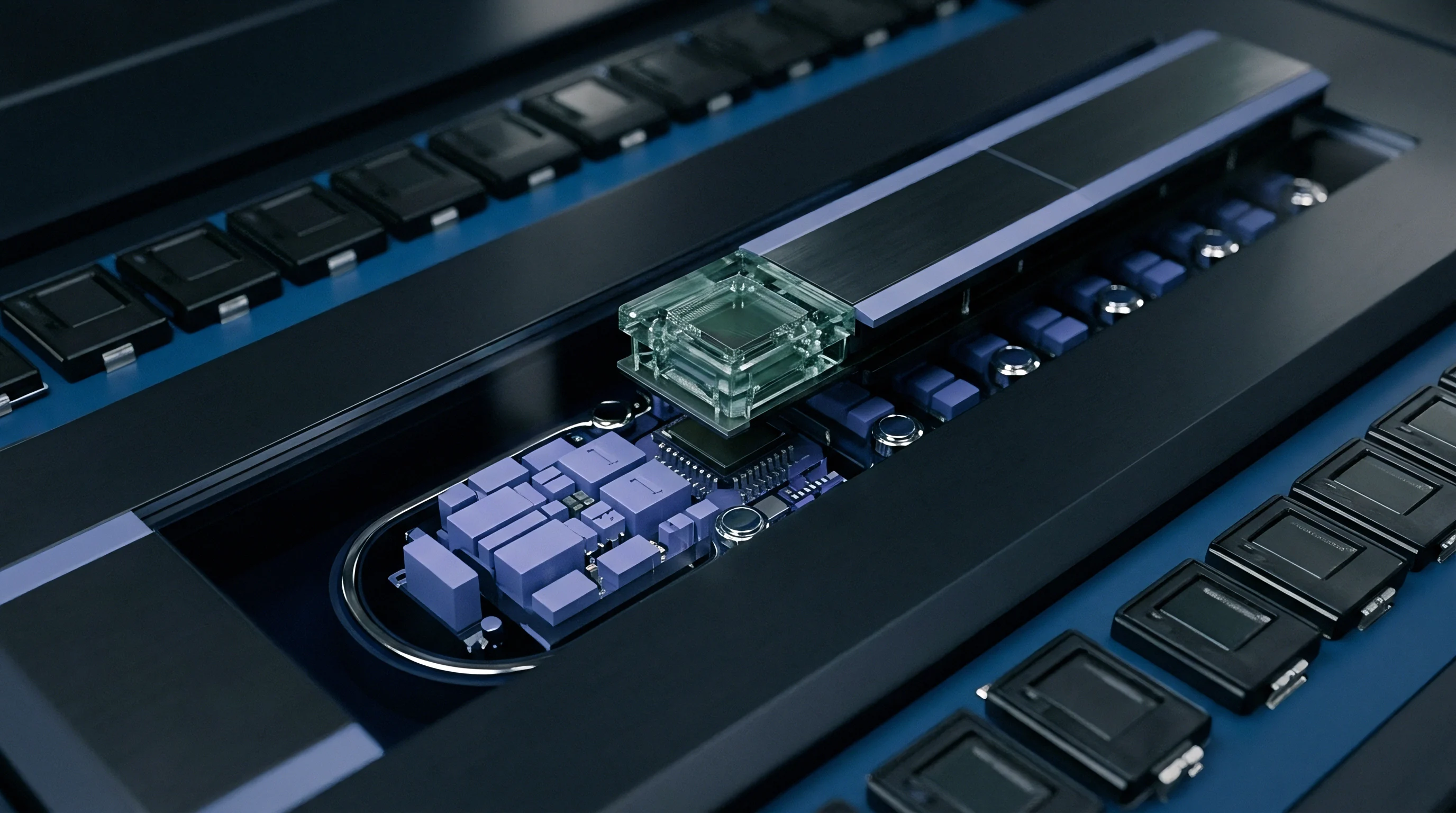
IPC/JEDEC-9704 specifies how sensors should be positioned near vulnerable BGAs and peripheral packages. Board bending places maximum tensile stress on the solder joints right under the outer corner spheres of a BGA. Placing the gauge as close to these corner balls as possible captures interfacial stresses before pad lifting happens, though real-world clearance often gets in the way.
Passives, keepouts, and conformal coating crowd high-density layouts, pushing the gauge center outward.
Rosette Orientation and Corner Offset
Corner solder balls take the heaviest load during four-point bending and handling. Placing a triaxial rosette requires accounting for the offset between the package corner and the center of the active grid. Ideally, the gauge edge sits within 1.0 millimeter of the package body, placing the grid center 2.0 millimeters plus or minus 0.2 millimeters from the corner joint.
Pushing that offset past 3.0 millimeters drops measured peak microstrain by twenty to forty percent, depending on laminate thickness and nearby ground planes.
Planar triaxial rosettes use three grids ~ channels 1, 2, and 3, or a, b, and c ~ set at 0 degrees, 45 degrees, and 90 degrees. Aligning the central 45-degree axis with the package corner bisector points the primary sensing axis toward the component center, catching the radial tensile gradient from the die shadow. Rotating this axis even fifteen degrees off-target skews principal angle calculations and artificially lowers peak strain readings during qualification.

Where Do Microstrain Concentrations Peak around Solder Joints?
When a board flexes downward, tensile stress concentrates between the copper land and the intermetallic compound layer. Perimeter solder balls along the sides face mostly pure shear, while corner balls experience combined shear and tension. Underfill alters this behavior: capillary underfill spreads mechanical shock across the full underside of the package, shifting peak surface strain past the fillet edge.
Without underfill, substrate flexure dumps directly into the corner solder ball, producing a sharp strain spike that decays within three laminate thicknesses of the package edge.
| Component Package Type | Grid Offset Distance | Laminate Thickness | Measured Strain Attenuation | Pad Fracture Detection Risk |
|---|---|---|---|---|
| BGA 1156, 1.0 mm Pitch | 1.2 mm | 1.6 mm | 8 percent | Low |
| BGA 1156, 1.0 mm Pitch | 2.5 mm | 1.6 mm | 27 percent | Moderate |
| BGA 1156, 1.0 mm Pitch | 4.0 mm | 1.6 mm | 49 percent | Severe |
| BGA 484, 0.8 mm Pitch | 1.0 mm | 1.0 mm | 12 percent | Low |
| BGA 484, 0.8 mm Pitch | 3.0 mm | 1.0 mm | 54 percent | Severe |
| QFN 64, 0.5 mm Pitch | 0.8 mm | 1.6 mm | 6 percent | Low |
Proper surface preparation is what keeps the gauge attached to the solder mask. Untreated solder mask is smooth and low-energy, which can lead to adhesive failure during sharp flex events. Lightly abrading with 400-grit silicon carbide paper and cleaning with isopropyl alcohol creates a matte surface that grips adhesive without damaging sub-surface copper.
Exposed FR-4 resin gives a stronger bond than prepared mask, but milling away solder mask creates local stiffness variations that alter strain patterns.
IPC/JEDEC-9704 requires test reports to record the exact coordinate offset of each rosette from the component edge to verify compliance with acceptance limits.

Excitation
Signal conditioning bridges translate small resistance shifts into digitized millivolts. At 1000 microstrain with a gauge factor of 2.0, a 120-ohm sensor shifts by just 0.24 ohms. Quarter-bridge setups rely on three completion resistors to form the Wheatstone bridge.
Precision networks inside instrumentation modules need resistance tolerances tighter than 0.05 percent and temperature coefficients under 5 ppm per degree Celsius; any drift inside the bridge circuitry registers as false mechanical strain.
A three-wire quarter-bridge arrangement cancels out lead resistance changes caused by temperature swings along cable runs. Two wires supply excitation voltage and bridge return, while a third sense line runs to the high-impedance amplifier input. Matching the lead lengths keeps resistance changes equal on opposing bridge arms.
Two-wire connections are unreliable on cable runs over five meters, where thermal gradients can cause artificial strain offsets above 150 microstrain.
A three-wire connection eliminates lead resistance drift when cables pass through oven drafts or hot spots inside enclosures.

Sampling Rates and Analog Filtering
Board assembly operations span vastly different time scales. Inserting a board into a fixture manually generates strain pulses over several hundred milliseconds. By contrast, depaneling saws, punch dies, and pneumatic routers generate shock transients with rise times under 200 microseconds.
Catching these short strain peaks requires continuous sampling on high-bandwidth acquisition hardware.
- Depaneling routers generate high-frequency vibration spikes that require sample rates of at least 10 kilo-samples per second per channel to capture true peak values.
- Connector insertion presses create quasi-static strain profiles that a 500 sample per second digitizer can capture accurately.
- Screw assembly torquing applies torsion and bending over two to five seconds; low-pass filtering at 100 Hertz is needed to strip out motor harmonic noise.
- Drop shock fixtures excite board resonances above 1500 Hertz, requiring analog anti-aliasing filters set at 10 kilo-Hertz with 50 kilo-sample per second converters.
Selecting excitation voltage means balancing signal strength against self-heating. Running 5 volts across a small 120-ohm grid dumps 52 milliwatts into an area under two square millimeters. Thin laminates cannot shed this heat quickly enough, leading to local resin softening under the gauge.
Modern instruments use pulsed excitation or lower voltages ~ typically 1.0 to 2.0 volts direct current ~ keeping heat under 10 milliwatts per gauge while resolving down to 0.5 microstrain with twenty-four-bit delta-sigma converters.
High-bandwidth interfaces can push strain telemetry deep into automated production lines, provided digital bus latency is kept low.
Envelope
Raw strain readings from triaxial rosettes are converted into scalar metrics to assess board damage risk during assembly. Data from the 0, 45, and 90 degree channels feed standard elasticity formulas to calculate maximum principal strain, minimum principal strain, and maximum shear for every sample point. Dynamic assembly steps bring strain rate into play as well.
Solder is sensitive to loading speed; under rapid deflection, it behaves brittely, transferring stress into the intermetallic layer rather than yielding plastically.

Will Dynamic Strain Rates Invalidate Static Limits?
Static strain limits do not protect boards during rapid mechanical shock. An assembly might sustain 1200 microstrain during slow handling without issue, but crater pads at just 600 microstrain under a pneumatic punch. Solder toughness drops fast as loading speeds increase.
At high displacement rates ~ around 10,000 to 100,000 microstrain per second ~ solder has no time to relieve stress through creep or grain boundary movement, leaving the nickel-tin or copper-tin interphase susceptible to clean cleavage.
IPC/JEDEC-9702 outlines how to calculate principal strains and test board interconnect reliability. Dynamic strain metrics for planar rosettes are derived using standard closed-form equations:
- Maximum principal strain calculates the highest tensile deformation in the board plane, regardless of direction.
- Minimum principal strain resolves the orthogonal compression occurring along the secondary axis.
- Principal angle determination tracks how the direction of peak tensile stress rotates relative to the component body during a stroke.
- Strain rate computation takes the time derivative of principal strain across sample intervals to spot sharp shock transients.
| Strain Rate (microstrain per second) | Standard Limit for 1.6 mm Board | Standard Limit for 1.0 mm Board | Permissible Diagonal Strain | Dominant Failure Mode |
|---|---|---|---|---|
| Below 1,000 | 950 microstrain | 700 microstrain | 800 microstrain | Ductile Solder Plasticity |
| 1,000 to 10,000 | 720 microstrain | 520 microstrain | 600 microstrain | Interfacial Cleavage |
| 10,000 to 100,000 | 500 microstrain | 370 microstrain | 420 microstrain | Pad Cratering and Trace Tear |
| Above 100,000 | 380 microstrain | 280 microstrain | 310 microstrain | Laminate Core Delamination |
Many packaging teams prefer diagonal strain metrics for evaluating BGA corners. This calculation isolates the strain vector running from the component corner toward its center ~ the path along which corner solder balls and pads usually fail. Evaluating both maximum principal strain and diagonal strain ensures complex torsional loading does not bypass simple scalar limits.
Calculating strain rate across a five-point moving window filters out electrical noise without dulling sharp mechanical shock peaks.
Thinner boards require stricter strain limits. For the same linear deflection, a 0.8-millimeter board bends to a tighter radius of curvature than a 2.4-millimeter board, forcing higher local shear between the rigid component die and the laminate. Heavy internal copper layers or ceramic cores also concentrate bending stresses at surface pads, reducing safe strain limits by thirty percent compared to standard eight-layer FR-4 stackups.
Exceeding dynamic strain limits during production often leaves latent solder cracks that pass ICT, only to fail later in the field.

Dispute
When BGA solder joints crack during production, liability disputes between OEMs and contract assemblers usually follow. Assemblers often point to flawed component batches or cramped board layouts, while brand owners blame misaligned ICT push pins, aggressive routing bits, or rough heat sink installation. Running strain measurement on the factory floor resolves these disputes with clear time-series data.

Fixture Qualification and Acceptance Sign-Off
Manufacturing service agreements routinely require strain gauge qualification for any tooling that contacts the board before lot sign-off. This applies to ICT nests, functional test fixtures, depaneling routers, odd-form placement nozzles, and final assembly jigs. Qualification involves running instrumented test boards ~ or pre-production units fitted with rosettes near every component larger than ten millimeters per side ~ through the process.
- Support pin layout errors are the main cause of ICT fixture failures, causing sharp local bending when vacuum pulls the board down.
- Hold-down gate misalignment applies concentrated point loads directly to package bodies instead of spreading force along bare board edges.
- Dull depaneling blades spike strain rates during tab breakout, often doubling peak displacement on nearby sensors.
- Manual connector insertion causes wide operator variance, where heavy thumb pressure routinely produces spikes over 1500 microstrain.
A standard qualification report includes time-series strain plots from at least five consecutive cycles per station. Tooling passes only if every channel stays within allowable strain envelopes across all five runs. If even one channel breaches the threshold, the fixture must be modified ~ repositioning support pins, slowing router feeds, or redesigning manual clamps ~ and the full five-cycle test rerun from scratch.
Short strain spikes during vacuum pull-down occur over milliseconds and are often tolerated when leadframes are sufficiently compliant.