
Piezoresistive Sensitivity Optimization in Ion Implanted Silicon Pressure Sensors
Ion implantation optimizes piezoresistive sensor sensitivity by balancing boron dose against gauge factor decay, junction depth, and thermal span stability.

Ion implantation optimizes piezoresistive sensor sensitivity by balancing boron dose against gauge factor decay, junction depth, and thermal span stability.

Time-temperature-moisture superposition predicts package-induced zero drift by shifting viscoelastic adhesive relaxation across temperature and humidity scales.

Optimal ASIC register tuning balances front-end gain against polynomial resolution, minimizing thermal offset and span drift across packaging stress limits.

Thermodynamically constrained Prony series parameterization models package viscoelastic relaxation, predicting and mitigating multi-year MEMS zero bias shift.
Polymer packaging stress relaxation shifts sensor zero-point calibration over time, requiring compliant submount isolation or factored field recalibration intervals.

Dynamic thermal cycling induces packaging adhesive creep and hysteresis that corrupt low-pressure piezoresistive accuracy unless isolated by multi-dwell testing.

Anodic bonded glass pedestals require aspect ratios above 1.25 and compliant submounts to decouple expansion shear strains from sensitive silicon diaphragms.

Anodic glass pedestals isolate silicon pressure sensors from packaging stress, locking thermal zero drift within 0.1 percent full scale across service life.
Viscoelastic mold compound relaxation and PCB flexure shift bandgap reference voltages via silicon piezoresistivity, demanding thermomechanical co-simulation.

Alkali drift and structural glass relaxation shift sensor zero-points over years; mitigating drift demands pre-aging bakes and barrier films.
Full-bridge piezoresistive layouts linearize strain response and reject thermal drift, while digital front-end packages shift line calibration into firmware.
Asymmetric PCB expansion forces differential shear across bandgap die pairs, requiring balanced land patterns and isolation slots to preserve millivolt precision.

Ductile metallic interlayers absorb anodic thermal contraction through plastic shear, cutting post-bond bow from 80 to under 20 micrometers on 150-millimeter stacks.

Packaging mold shrinkage and board reflow solder strain alter silicon bandgap voltages via piezoresistive coupling, demanding compliant leads or ceramic packages.

Anisotropic silicon strain tensors corrupt precision converter references; selecting compliant leadframes or ceramic cavities prevents uncorrectable drift.

Mitigate anodic bonding residual stress by matching CTE crossover points and cooling at under 1°C/min to prevent sensor zero-point drift.

Dynamic PCB thermal bending moments induce false piezoresistive bridge drift that layout slots, compliant leadframes, and synchronous sampling resolve.

Calculating real operating distance across non-ferrous alloys relies on multiplying nominal range by reduction factors set by target conductivity and skin depth.

Standard inductive target specifications demand an Fe 360 square plate sized to the face diameter or three times nominal range to assure rated trip points.

Helium permeation through borosilicate glass and electrochemical hydrogen evolution limit cavity life, requiring thin-film barriers and non-evaporable getters.

Milled PCB isolation slots and compliant leaded packages attenuate board-level thermal gradient strain to preserve 24-bit converter offset accuracy.

Intermetallic growth stiffens the solder substrate interface, converting creep strain into high interfacial shear stresses that accelerate thermal fatigue failure.

Minimize parasitic light sensitivity using deep trench isolation, tungsten shielding, and optical bandpass filters to isolate storage nodes from continuous ambient light.

Nanosecond pulsed illumination demands sub-nanohenry loop inductances and Kelvin gate returns to deliver stable multi-ampere optical strobe pulses.
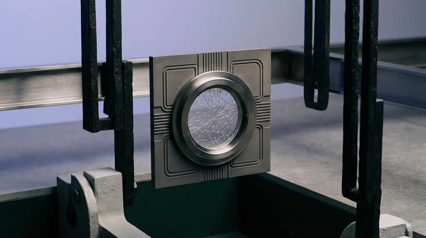
Standard micro cavity vacuum assessment requires non-destructive optical lid deflection or resonant Q-factor testing to bypass sub-nanoliter volume limits.
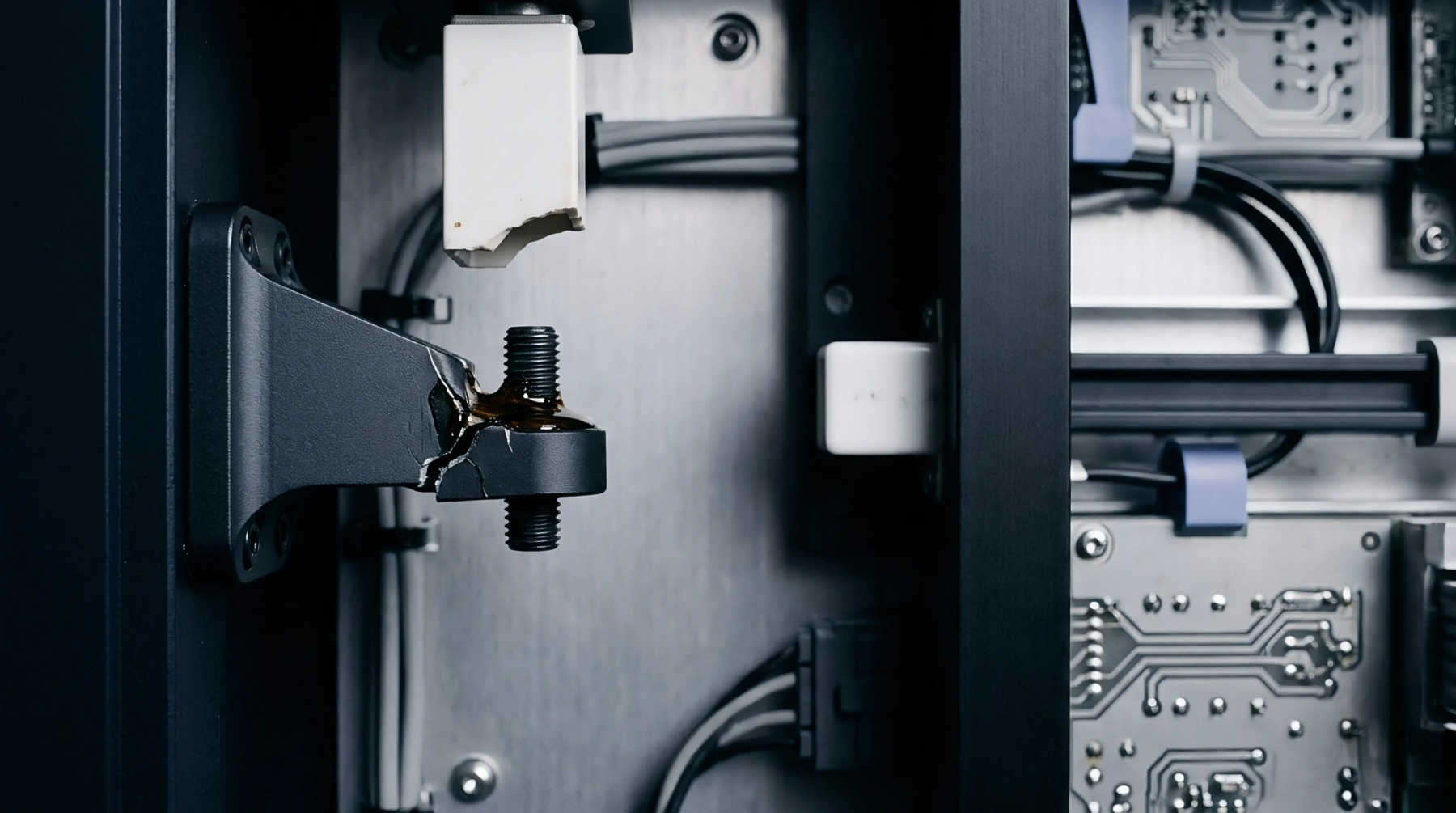
Calculate viscoelastic stress transfer by fitting multi-mode Prony series DMA data and applying Arrhenius-corrected shift factors under thermal cycling dwells.

Global Reset Mode clears all pixel photodiodes simultaneously, requiring synchronized light strobing or mechanical shuttering before row readout starts to avoid exposure gradients.

Distributed interconnect parasitic capacitance limits row line switching speed, demanding full 3D extraction to prevent array settling errors.

Characterize horizontal line timing by synchronizing direct row-driver probing with output packet decoding to decouple RC trace delays from ADC conversion phases.

Evaluating getter activation temperatures balances thin-film oxide dissolution kinetics against wafer bonding thermal budgets to prevent cavity pressure drift.
Expertise is a utility, not a secret. sentiention™ publishes its working knowledge as open reference: intelligence layer covering the materials it sources, the markets it enters, and the reference that serves both.