Piezoresistive Sensitivity Optimization in Ion Implanted Silicon Pressure Sensors
Ion implantation optimizes piezoresistive sensor sensitivity by balancing boron dose against gauge factor decay, junction depth, and thermal span stability.
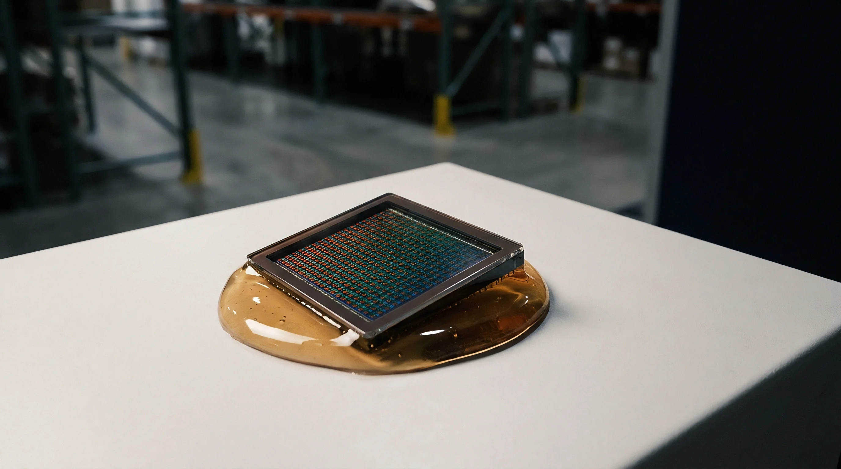

Profile
Piezoresistive sensitivity in silicon pressure sensors depends heavily on the depth profile of electrically active dopants. For p-type resistors on n-type (100) silicon, boron or boron difluoride is typically implanted through a thermal silicon dioxide screen oxide. The piezoresistive coefficient along the <110> crystallographic axis sets the fractional change in resistance under mechanical stress.
At low surface acceptor densities below 1017 cm-3, the room-temperature shear coefficient approaches its theoretical limit near 138 × 10-11 Pa-1. Higher implant doses increase carrier concentration, dampening stress response through carrier screening and intervalley scattering accounted for by the Kanda factor.
Designing for span sensitivity forces an unavoidable compromise. While a light implant yields high gauge factors, the accompanying high sheet resistance elevates thermal noise and the thermal coefficient of resistance. It also raises sensor output impedance, leaving the bridge vulnerable to electromagnetic pickup and humidity-induced drift.
Implantation energy determines the projected range and straggle of the dopant, defining how thick the piezoresistive layer ends up relative to the bending diaphragm surface.
Because boron forms shallow acceptor states, keeping the active resistor within the top 200 nanometers of the diaphragm maximizes coupling to peak surface stresses under differential pressure loading. Deeper junctions dilute the measured strain as the lower portion of the implanted well reaches into the lower-stress neutral planes of the plate.
Boron implantation at 40 keV with a dose of 2 × 10¹⁴ ions per square centimeter yields a longitudinal piezoresistive coefficient of 62 × 10-11 Pa-1 at 25 degrees Celsius.
Characterizing these implanted layers requires separating sheet resistance from carrier mobility and electrical activation. Four-point probe maps across a 200-millimeter wafer show sheet resistance variations that track directly with bridge offset voltage and span spread. Secondary ion mass spectrometry measures total chemical boron, while spreading resistance profiling maps the active carrier distribution following thermal activation.
Gaps between total chemical dopant and active density reflect incomplete lattice substitution and transient enhanced diffusion.
| Implant Species | Energy (keV) | Dose (cm-2) | Peak Density (cm-3) | Sheet Resistance (Ohm/sq) | Longitudinal Gauge Factor | TCS (ppm/K) |
|---|---|---|---|---|---|---|
| B11 | 30 | 1.5 × 10¹⁴ | 1.2 × 10¹⁸ | 380 | 74 | -1850 |
| B11 | 45 | 5.0 × 10¹⁴ | 3.8 × 10¹⁸ | 165 | 58 | -1420 |
| BF2 | 40 | 1.0 × 10¹⁵ | 8.5 × 10¹⁸ | 110 | 46 | -1080 |
| BF2 | 60 | 3.0 × 10¹⁵ | 2.4 × 10¹⁹ | 62 | 31 | -650 |
Balancing sensitivity against thermal drift requires selecting dose windows that constrain the temperature coefficient of sensitivity. Once the chemical dose exceeds 5 × 1015 cm-3, the piezoresistive factor drops below half its intrinsic value, complicating signal conditioning for low-pressure ranges below 100 kilopascals.
- Target sheet resistance establishes the baseline bridge resistance and fixes the Johnson noise floor for low-noise instrumentation amplifiers.
- Screen oxide thickness alters the true penetration depth of incident ions, requiring spectroscopic ellipsometry qualification before batch processing.
- Substrate orientation accuracy maintains alignment with the <110> direction within 0.5 degrees, preventing cross-axis shear sensitivity from corrupting differential pressure readings.
- Channeling suppression tilt limits axial crystal channeling during low-energy boron introduction, typically locked at an angle of 7 degrees with a 22-degree twist.
If dopant distribution varies by more than five percent across the wafer, electronic calibration trim ranges must expand, eroding yields and worsening zero-point thermal error.

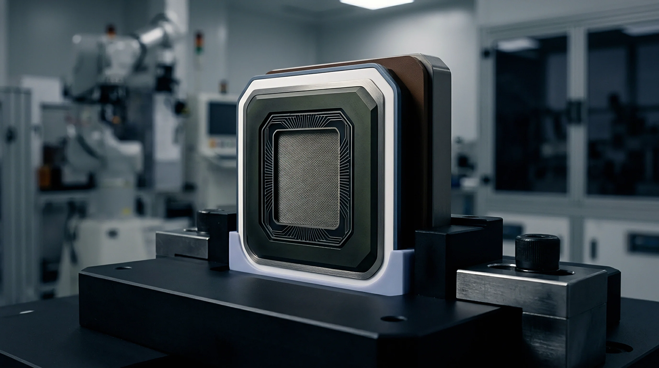
Mask
Photolithographic patterning defines the planar geometry, placement, and orientation of the gauges across the diaphragm. In a square clamped diaphragm, mechanical stress peaks at the center of the clamped edges, where aligning the resistor’s longitudinal axis along the <110> direction yields the highest piezoresistive coefficient. Even a rotational misalignment of two degrees lowers the effective coefficient by several percent, causing an immediate sensitivity loss across the run.
Resistor dimensions define how the localized stress field averages out across the element, even when heavier ions limit crystal channeling. If a resistor layout extends too far toward the diaphragm center, its outer segment captures peak tensile stress while the inner segment sits in regions of decaying or reversed stress. This geometric integration dilutes the net resistance change and reduces full-scale span.
Layouts generally keep lengths under 100 micrometers and widths above 4 micrometers so lithographic edge roughness does not dominate resistor tolerance.
Heavier dopant atoms narrow the active strain zone while raising junction barrier capacitance.
Alignment tolerances between the backside-etched cavity and the frontside resistor implants govern zero-pressure bridge offset, regardless of how implant screens absorb low energies. Infrared backside alignment tools typically hold positioning errors below 1.0 micrometer. Any lateral shift between the diaphragm edge and the resistor array exposes opposing bridge arms to asymmetric stress, producing non-linear response curves and zero-offset drift under cyclic loading.

Is Mask Misalignment Measurable across Bridge Asymmetry?
Bridge imbalance at wafer level helps separate alignment errors from chemical dose gradients. A pure sheet resistance gradient causes a monotonic shift across all four bridge legs. By contrast, backside mask misregistration places opposing resistors at unequal distances from the stress peak, generating a differential resistance error proportional to pressure.
By comparing zero-pressure offset with full-scale span differentials, placement errors can be distinguished from diffusion gradients even when wafer warping skews lithographic targets.
Contact opening layout controls current crowding, and contact resistance directly degrades bridge balance. The transition between the lightly doped resistor channel and the heavily doped contact diffusion introduces parasitic resistances that do not respond to diaphragm stress. If contact overlap varies across the die through mask run-out, this inactive series resistance alters the sensitivity of individual bridge arms and undermines common-mode rejection.
Locating piezoresistors within the steep stress gradient at the diaphragm edge demands lithographic registration tighter than the junction depth itself.
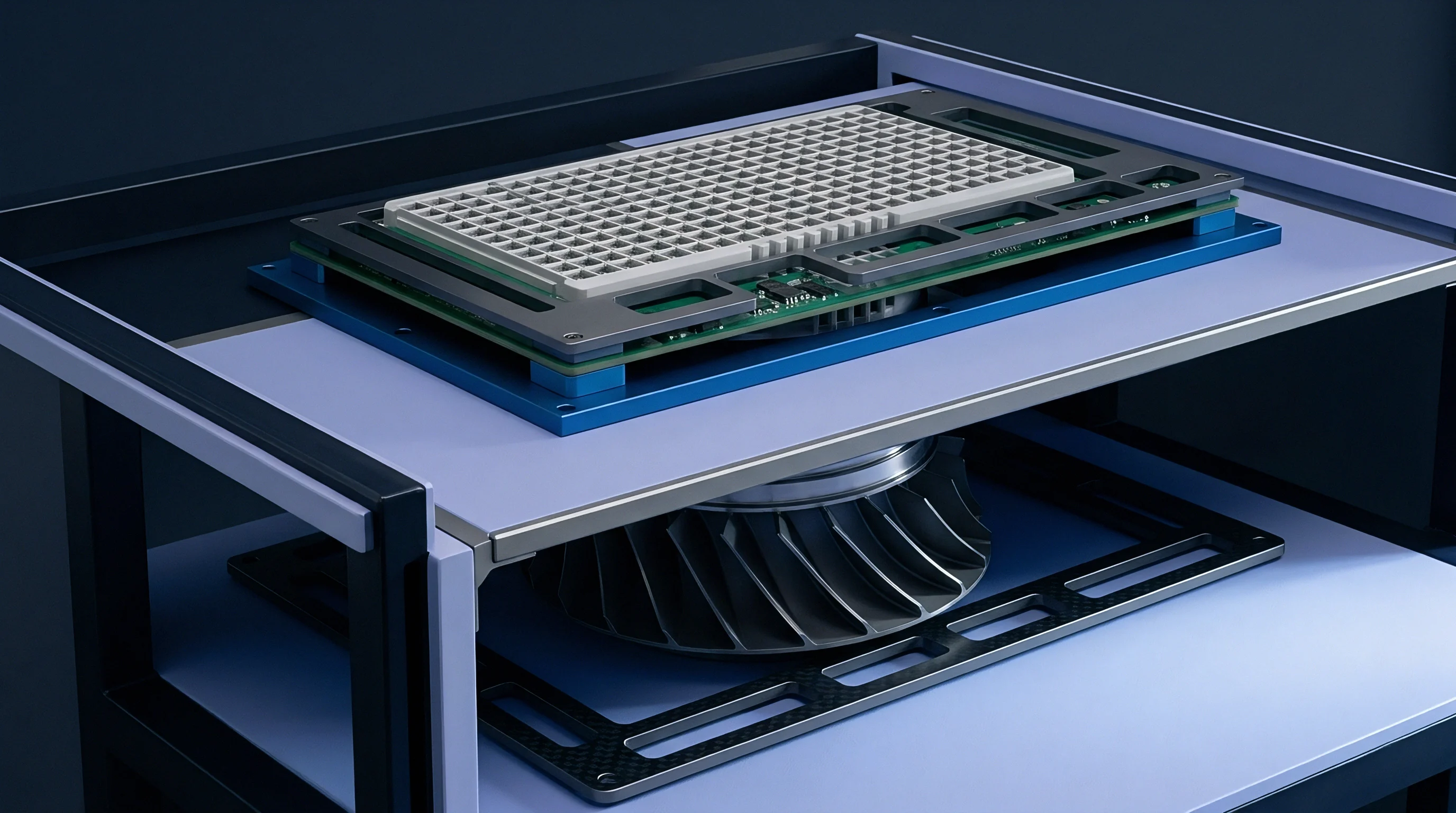
Anneal
Thermal processing repairs lattice damage from ion bombardment and drives implanted impurities into substitutional sites before defect clusters pin mobile carriers. Rapid thermal processing relies on tungsten-halogen lamps to ramp past 1000 degrees Celsius at over 50 degrees per second, activating dopants while curbing transient enhanced diffusion from silicon self-interstitials. In contrast, furnace annealing at 900 degrees Celsius for 30 minutes broadens the profile, driving the p-n junction deeper into bulk silicon where diaphragm bending stress falls off.
Junction depth dictates edge placement, while boron atoms resting in non-substitutional sites act as neutral scattering centers rather than acceptors, degrading carrier mobility without contributing to piezoresistance. Electrical activation must exceed 95 percent to guard against long-term resistance drift at elevated operating temperatures.
Because thermal budgets dictate final diffusion, incomplete annealing leaves vacancy-interstitial complexes in the junction depletion region. These defects serve as generation-recombination centers that drive up reverse bias leakage. Above 85 degrees Celsius, that leakage shunts the piezoresistor channel, causing zero-point drift and span loss.
- Transient interstitial diffusion causes anomalous profile broadening, shifting the junction depth beyond the nominal computer-simulated boundary.
- Point defect clustering traps mobile holes, generating low-frequency flicker noise that obscures sub-pascal pressure fluctuations.
- Surface oxide stress induction alters residual surface strain, modifying initial bridge offset voltages prior to pressure application.
- Precipitate formation occurs when peak concentrations exceed solid solubility limits, establishing localized leakage pathways across the isolation boundary.
Broad span tolerances typically stem from thermal furnace temperature non-uniformity across quartz tube heating zones.

Span
Assessing sensitivity requires analyzing full-scale output voltage against excitation and applied pressure. Bridge sensitivity S expresses millivolts of output per volt of excitation per unit pressure. On a square diaphragm of side length 2a and thickness h under uniform pressure P, edge stresses follow standard plate mechanics: longitudinal stress sigma_l runs parallel to current flow, and transverse stress sigma_t runs perpendicular to it.
A concrete calculation shows how mechanical strain converts to electrical output. Consider a square diaphragm with an edge length of 1000 micrometers and a thickness of 25 micrometers under a full-scale pressure of 100 kilopascals. Edge surface stress follows small-deflection plate theory:
sigma_edge = 0.308 × P × (2a / h)2
Evaluating this expression gives an edge stress of 49.3 megapascals. For p-type piezoresistors oriented along <110> on a (100) plane, the longitudinal coefficient pi_l equals 0.5 × pi_44, and the transverse coefficient pi_t equals -0.5 × pi_44. At an implant dose producing a pi_44 value of 90 × 10-11 Pa-1, the coefficients are pi_l = 45 × 10-11 Pa-1 and pi_t = -45 × 10-11 Pa-1.
The fractional change in resistance for the longitudinal resistor computes as:
Delta R_l / R = pi_l × sigma_l + pi_t × sigma_t
At the diaphragm edge, transverse stress couples to longitudinal stress through Poisson’s ratio nu, which is 0.06 along the <110> direction in silicon. Transverse stress is therefore 2.96 megapascals, giving a fractional resistance change of:
Delta R_l / R = (45 × 10-11 × 49.3 × 106) – (45 × 10-11 × 2.96 × 106) = 0.02218 – 0.00013 = 0.02205
For a fully active bridge with four matched resistors ~ two under tension and two under compression ~ differential output normalized to excitation V_in is:
V_out / V_in = Delta R / R = 22.05 mV/V
With 5.0-volt regulated excitation, full-scale span reaches 110.25 millivolts. Verifying this performance requires separating piezoresistive response from packaging stress through sequential calibration steps.
- Mount the unencapsulated die onto a ceramic header using low-stress silicone elastomeric adhesive.
- Place the test assembly into an automated pressure controller chamber referenced to a deadweight piston gauge traceable to national standards.
- Apply pressure points at 0, 20, 40, 60, 80, and 100 percent of nominal full scale at a stabilized ambient temperature of 20 degrees Celsius.
- Record bridge output voltages with an 8.5-digit digital multimeter possessing input impedance above 10 gigaohms.
- Calculate non-linearity errors using terminal point definitions in accordance with IEC 61298-2.
Procurement specifications referencing IEC 61298-2 clause 6.1 enforce terminal-based sensitivity calculations that disqualify raw best-fit straight line claims.
| Profile Identification | Implant Species | Nominal Bridge Span (mV/V) | Output Impedance (kOhm) | Noise Floor (nV/rtHz) | Zero Offset (mV/V) | Span Drift (%FS/yr) |
|---|---|---|---|---|---|---|
| Low-Dose Shallow | B11 (30 keV) | 28.5 | 4.2 | 8.3 | ±2.1 | 0.45 |
| Medium-Dose Balanced | B11 (45 keV) | 22.1 | 1.8 | 5.4 | ±0.9 | 0.18 |
| High-Dose Deep | BF2 (60 keV) | 14.2 | 0.7 | 3.4 | ±0.4 | 0.08 |
Procurement contracts that specify high bridge sensitivity without bounding Johnson noise force designs toward high-impedance, lightly doped channels that fail signal-to-noise checks in electrically noisy environments.


Balance
Thermal stability depends on balancing the temperature coefficient of resistance against the temperature coefficient of sensitivity. Lattice vibrations increasingly scatter charge carriers as temperature rises, driving down the piezoresistive coefficient and yielding a negative temperature coefficient of sensitivity. Over the same range, bulk resistance in the doped silicon climbs, producing a positive temperature coefficient of resistance.
When powered by a constant current rather than constant voltage, this rising resistance increases bridge voltage, compensating intrinsically for the dropping gauge factor.
Because sheet resistance tracks acceptor concentration, constant-current compensation works only when the temperature coefficient of resistance matches the absolute magnitude of the temperature coefficient of sensitivity. Achieving that balance requires holding active carrier concentration between 3 × 1018 cm-3 and 8 × 1018 cm-3. Outside this window the two curves diverge, forcing designs to rely on external thermistors or polynomial correction in an application-specific integrated circuit.

Will Deep P-Well Implantation Suppress Thermal Wander?
Dielectric isolation changes thermal drift behavior considerably. Resistors junction-isolated within an n-type epi layer suffer reverse leakage across the p-n barrier at higher temperatures. Deep p-well implants curb this leakage by widening the space-charge region, though they thicken the mechanical cross-section and reduce stress coupling.
Silicon-on-insulator designs replace the junction barrier with buried silicon dioxide altogether, eliminating substrate leakage up to 250 degrees Celsius at the expense of higher raw wafer costs.
- Passive span compensation resistors inserted in series with the excitation loop attenuate thermal sensitivity decay by dropping voltage as bridge resistance climbs.
- Zero-offset trim networks etched from thin-film nickel-chromium or polysilicon correct initial fabrication bridge imbalances.
- Laser trimming algorithms execute automated resistance balancing under controlled ambient conditions prior to hermetic sealing.
- Passivation nitride balancing balances compressive and tensile dielectric films, preventing thermal hysteresis from bending the diaphragm across thermal cycles.
Whether passive metallurgical networks can preserve bridge balance over ten years of continuous operation without developing contact electromigration drift remains an open question in field deployments.

Audit
Incoming inspection checks whether received lots meet specified accuracy, drift, and sensitivity limits before entering assembly. Sampling plans follow ISO 2859-1 normal inspection levels. Die-level wafer screening relies on probe cards with integrated pressure-port chucks to pulse differential pressures while logging output.
Zero offset, full-scale span, input impedance, and insulation resistance define the core receiving baseline.
Accelerated life testing quickly flags unstable dopant profiles or poor surface passivation. Running sample lots for 1000 hours at 125 degrees Celsius under full operating pressure reveals unannealed lattice damage, mobile ion migration, and junction breakdown. Referencing these tests against a pressure standard with an expanded uncertainty of 0.01 percent of reading ensures verification data reflects actual physical response rather than vendor curve fitting.
| Parameter | Test Method | Acceptance Limit | Sample Size | Rejection Consequence |
|---|---|---|---|---|
| Bridge Span Sensitivity | IEC 61298-2 Step Pressure | 22.0 ± 1.5 mV/V/bar | 100% Wafer Probe | Wafer Sort Binning Reclassification |
| Zero Pressure Offset | Zero Applied Differential | ±1.0 mV/V | 100% Wafer Probe | Laser Trim Rework |
| Thermal Sensitivity Shift | Thermal Chamber (-40 to 125 C) | < 0.05% Span/K | 5 dies per wafer | Lot Quarantine and Process Audit |
| High-Temp Storage Drift | 1000 hr at 125 C (IEC 60068-2-2) | < 0.2% Span Wander | 3 dies per lot | Entire Ingot Batch Rejection |
| Substrate Isolation Leakage | 50V Reverse Bias at 85 C | < 10 nA | 100% Wafer Probe | Scrap Defective Wafers |
Wafer-to-wafer sheet resistance variation directly dictates trim cycle times on the line. Supply agreements assign clear financial liability for out-of-spec lots discovered during surface-mount assembly. When qualification records prove that dies drift beyond annual stability limits within the first quarter of operation, warranty clauses pass recalibration and scrap expenses back to the foundry.
Robust incoming controls protect factory yield and keep intrinsic silicon behavior distinct from downstream packaging artifacts.