Metrology Standard
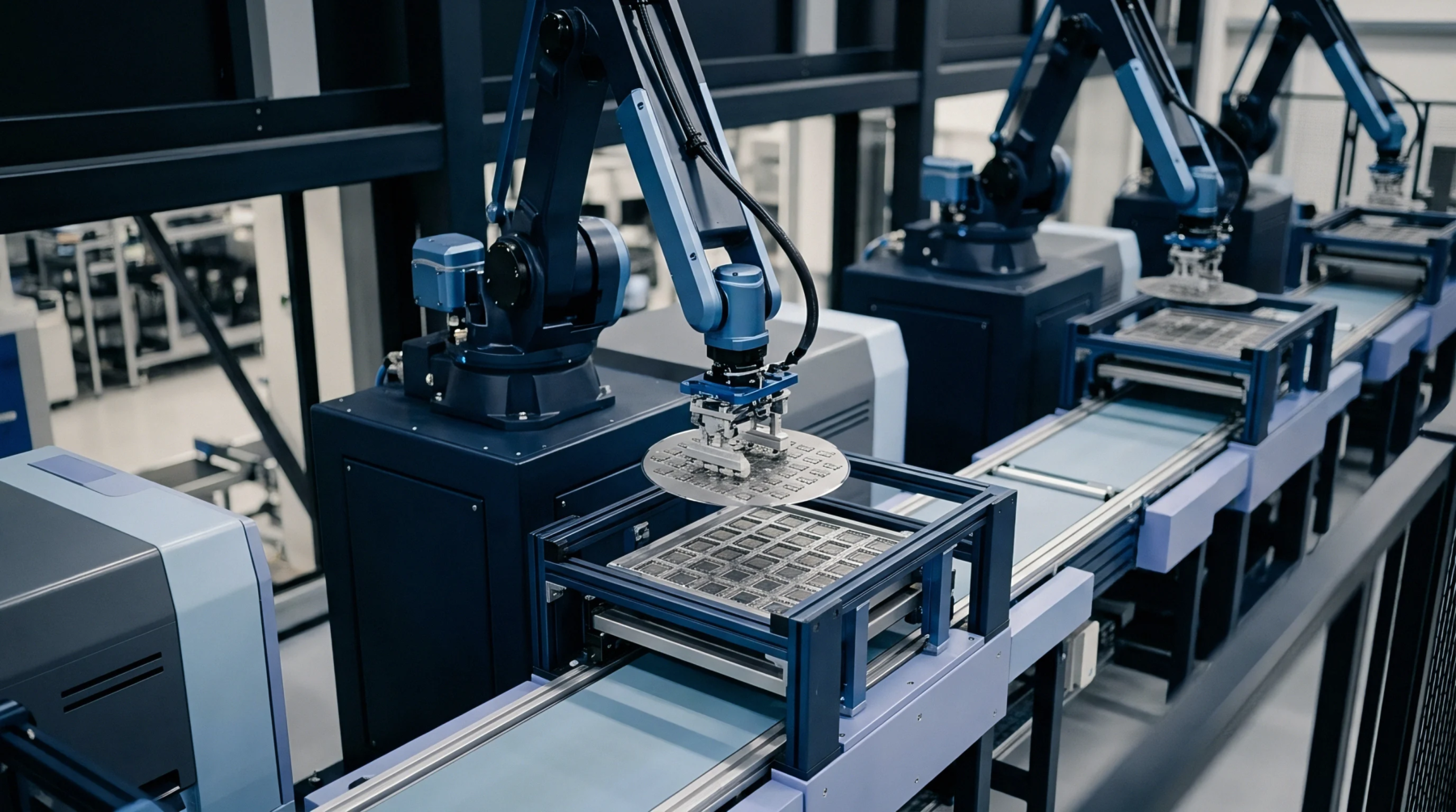
Silicon wafer manufacturing requires standardized procedures to determine total thickness variation and surface curvature parameters across polished substrates. Semiconductor fabrication facilities rely on unified measurement protocols to ensure automated material handling equipment compatibility. Standardized test methods established under SEMI MF1451 specify non-contact dimensional measurement techniques for silicon wafers used in microelectronic device manufacturing.
Automated wafer sorting tools implement these procedures to verify geometry prior to high-density photolithography processing.
Thickness Verification
Dual-probe capacitive measurement systems evaluate wafer thickness by measuring distance gaps between upper and lower sensors while the substrate rests on air bearings. Differential capacitance measurements eliminate position errors caused by vertical wafer float between non-contact sensing heads. Environmental temperature control within zero point one degree Celsius prevents thermal expansion errors in sensor mounting fixtures.
Spatial sampling grids evaluate hundreds of surface points to compute maximum thickness variation across full wafer diameters.
Optical Principle
Laser displacement sensors offer alternative non-contact height measurement capabilities, utilizing triangulation algorithms to map upper and lower wafer surfaces. Surface reflectivity changes require dynamic sensor gain adjustment to maintain distance measurement resolution across variable surface coatings.
Calibration Artifact
Traceability relies on certified master reference wafers with certified thickness profiles calibrated by national measurement institutes.