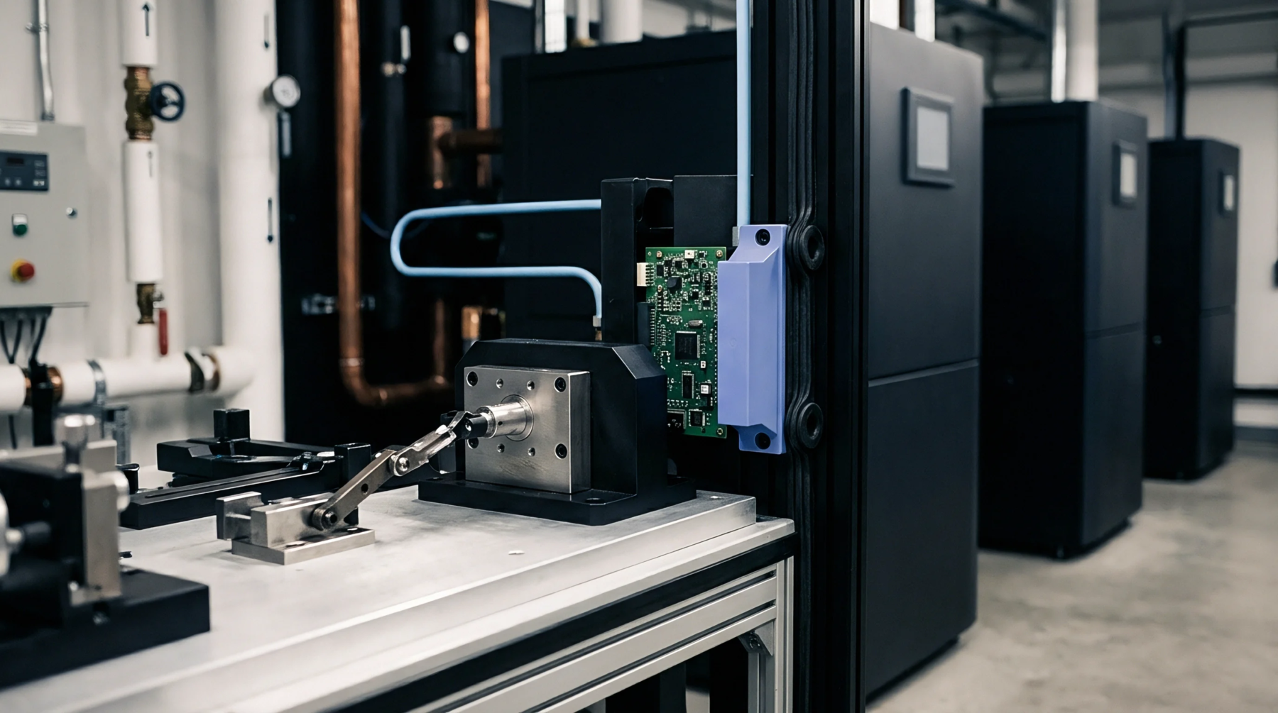
Board Flex Reaching the Die as Offset Error after Assembly
Board flexure transfers shear strain through solder joints into silicon dies, shifting zero-point offsets; isolate footprints using slots or diagonal placement.
Board flexure transfers shear strain through solder joints into silicon dies, shifting zero-point offsets; isolate footprints using slots or diagonal placement.
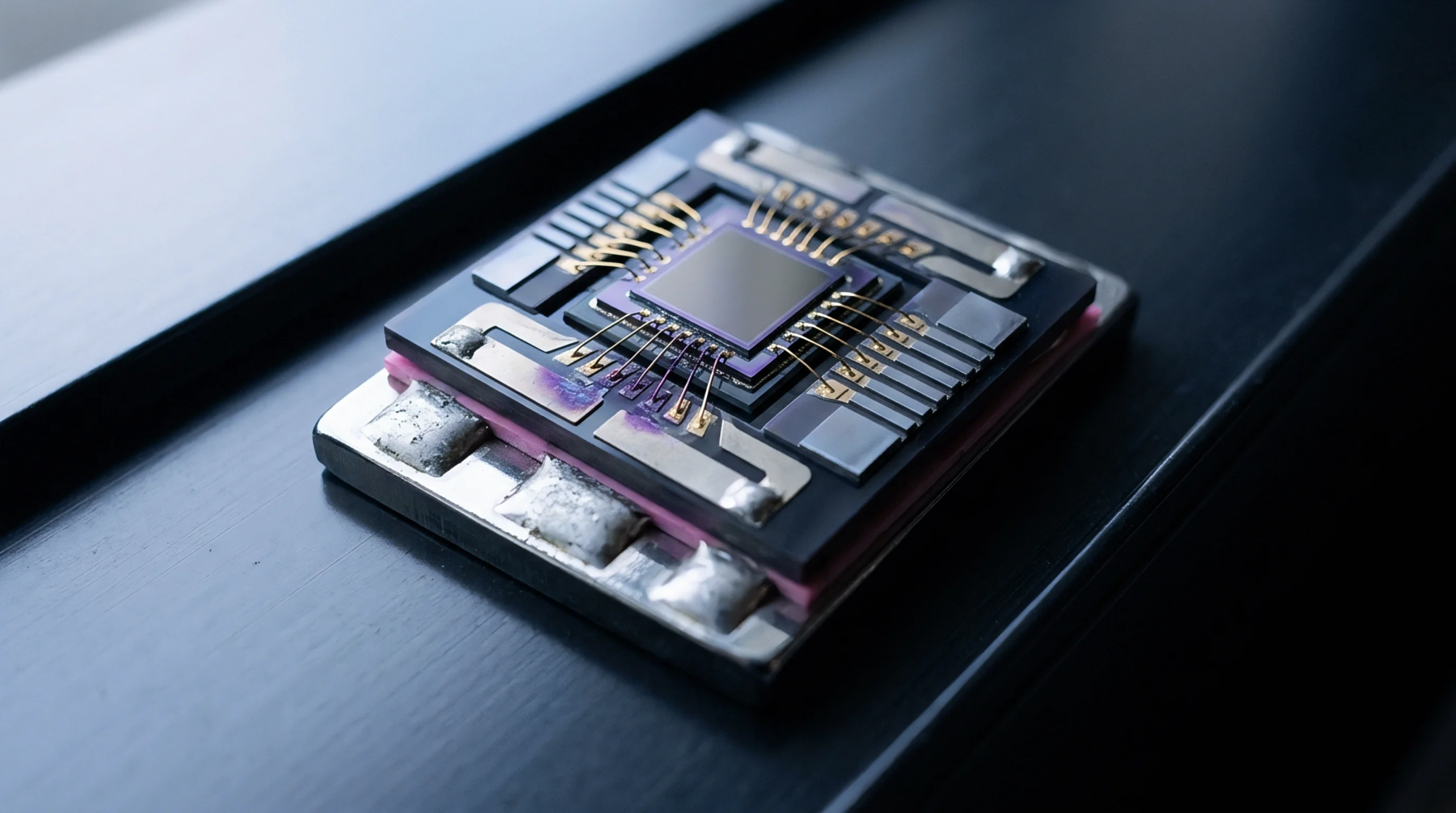
When component vendors end leaded packages, identical active silicon dies often survive in surface-mount forms that demand revised land patterns and thermal layouts.

Selecting die packaging forms requires matching land pattern mechanical stress, bus wiring distance, and calibration stability against landed unit economics.
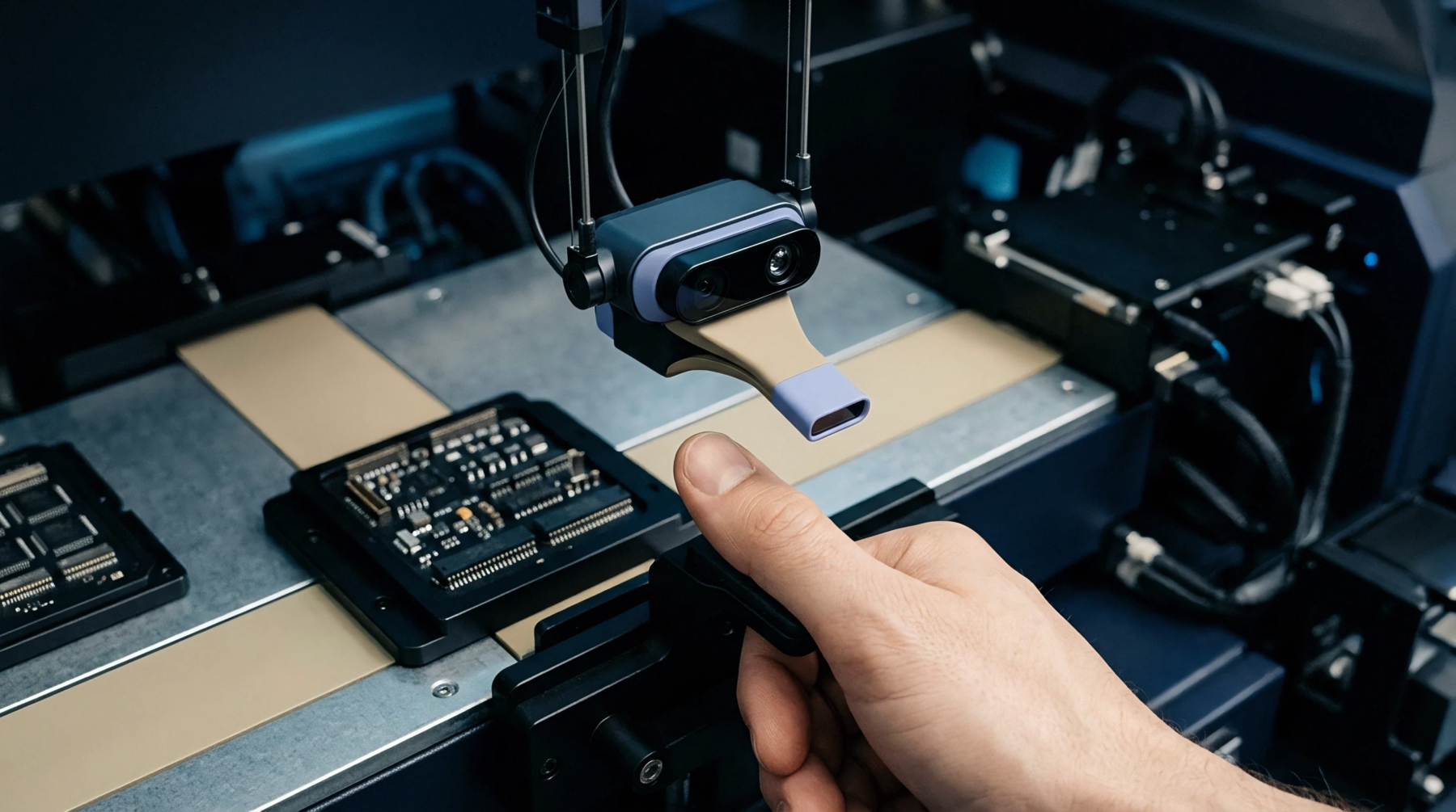
Precision land pattern design balances component manufacturing tolerances against board assembly capability to eliminate thermomechanical stress on silicon die output registers.

Iso-die package selection dictates backend lead times from 4 to 20 weeks and MOQs up to 50k units, requiring total landed cost models over raw component price.
Enforce 18-month EOL notice timelines and silicon-level allocation guarantees to protect sensor supply chains from unannounced component discontinuances.

Board level thermal gradients shift internal bandgap voltages by inducing transistor temperature differentials and piezoresistive package stress.

Land pattern geometry, bus capacitance control, and driver timing dictate assembly yield and operational stability across sensor package formats.

Dynamic address assignment eliminates multiplexers in dense sensor arrays through cascade enable lines or software ARP, reducing PCB area while raising firmware bring-up requirements.

Wafer level sensor package strain mitigation relies on compliant redistribution layers, optimized pad geometries, and firmware offset calibration to ensure operational stability.
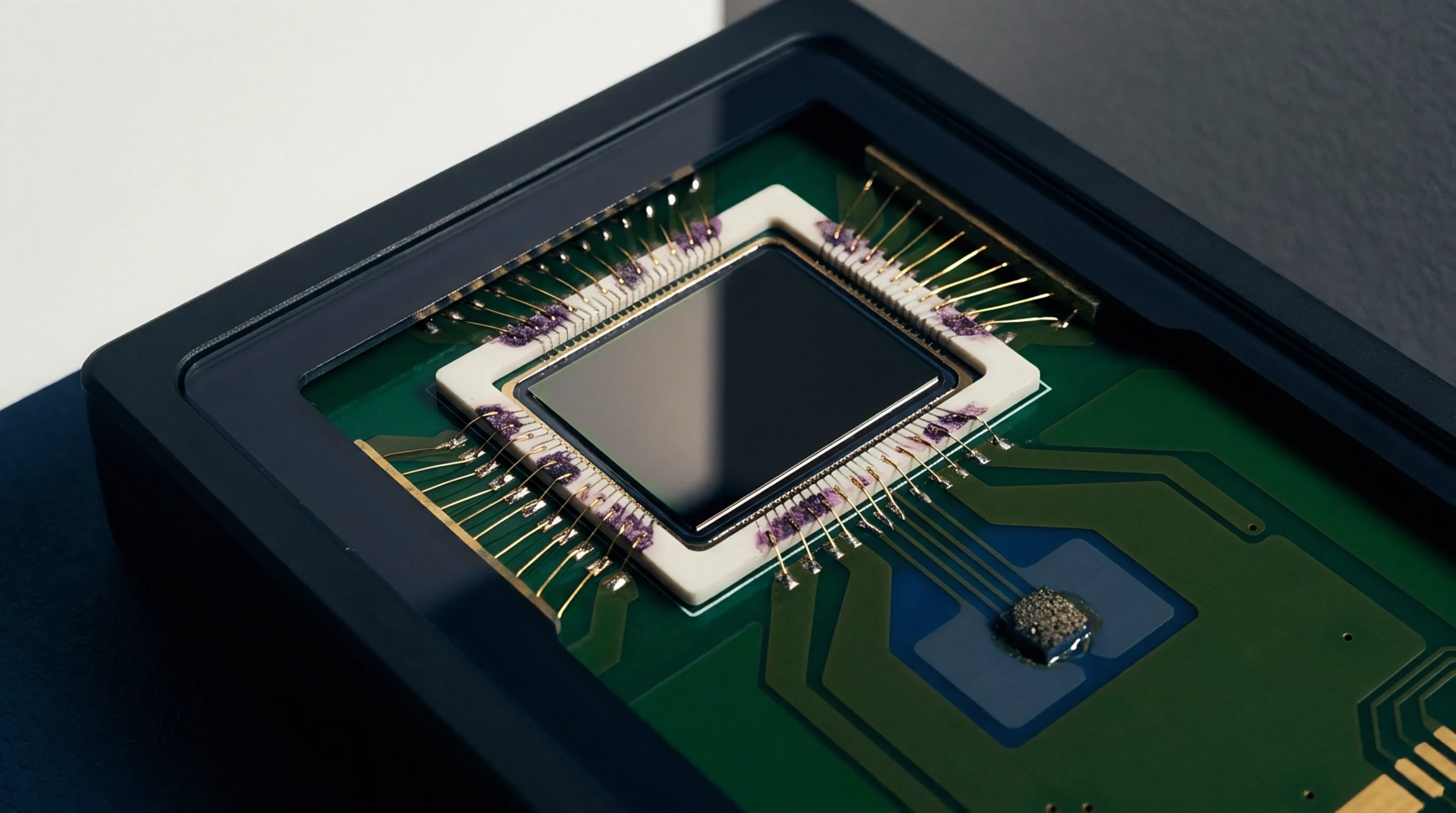
WLCSP packages transfer board thermal strain directly to the die, causing reference drift, while ceramic cavity housings eliminate mechanical coupling.

Wafer bank conversion agreements convert raw iso-die into multi-form sensor packages, shifting supply risk while managing lead time, yield, and bus drift.

Fine-pitch iso-die variants exhibit divergent zero-point offset drift governed by package compliance, substrate CTE mismatch, and mechanical piezoresistive stress transfer.

Structure IC orders using exact full-reel increments matching historical baseline entitlements to bypass automated shortage allocation cuts.

Static thermal zero-g bias shifts in MEMS accelerometers are isolated by enforcing prolonged thermal dwell periods to decouple stress creep from thermal gradients.
Board flexure stress couples to analog dies via solder joints and mold compounds, shifting bandgap voltages up to 10 millivolts under thermal cycling.
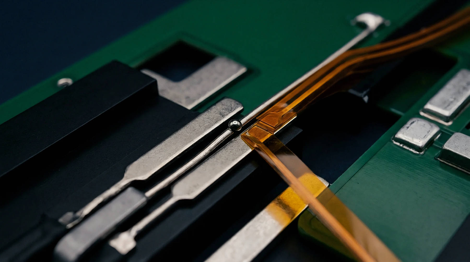
Dynamic PCB thermal gradients cause substrate flexing that alters converter resistor ladder ratios via piezoresistive strain, driving gain drift.

Asymmetric thermal expansion shifts bandgap voltage via piezoresistive substrate stress; mechanical slots and ceramic packaging isolate critical reference nodes.

Fine-pitch package assembly requires pairing stencil foil reductions with thin outer-layer dielectrics to maintain solder transfer and controlled impedance.
Thermomechanical fatigue modeling for WLCSP solder arrays requires mapping viscoplastic Anand strain energy density to predict field thermal cycling failures.

Multi-channel sensor integration on standard two-wire buses demands balancing parasitic bus capacitance, address resolution, layout geometry, and landed unit cost.

Quantifying timing budget degradation across multi-channel I2C switches requires auditing accumulated branch capacitance against pull-up rise time limits.

Mitigate bandgap thermal stress errors using compliant leaded packages, PCB isolation slots, polyimide die buffers, and stabilized factory calibration.
WLCSP packaging induces mechanical stress gradients that shift bandgap references, requiring rotated common-centroid layouts and active digital trim.

Characterizing substrate interface viscoelastic shear relaxation prevents dynamic thermal offset drift and avoids expensive late stage packaging redraws.

Bottom terminated package parasitic isolation requires thermal pad segmentation while mechanical stress drift is suppressed by limiting solder voiding under 10 percent.

Accumulated line capacitance degrades open-drain rise times, demanding active acceleration or branch buffering to maintain deterministic software enumeration.

Thermally isolates precision references from high-current output stages using symmetrical isometric layout, separate Kelvin return paths, and stress slots.
Thermal dissipation cycles induce package strain that skews bandgap reference outputs, necessitating symmetrical copper relief and strain-matched packaging.

Discrete surface mount sensors minimize unit costs at high volume but demand board space, assembly controls, and firmware bring-up that modules eliminate.
Expertise is a utility, not a secret. sentiention™ publishes its working knowledge as open reference: intelligence layer covering the materials it sources, the markets it enters, and the reference that serves both.