Minimum Order Allocation Algorithms during Integrated Circuit Shortage Cycles
Structure IC orders using exact full-reel increments matching historical baseline entitlements to bypass automated shortage allocation cuts.


Rationing
When semiconductor supply tightens, purchase order processing stops functioning as straightforward logistics and becomes an automated mathematical filter. Chip manufacturers deploy allocation engines inside their ERP systems to manage order books that routinely run three to five times above total wafer fab capacity. These algorithms weigh every incoming line item against historical consumption, account tiering, order velocity anomalies, and existing lead-time backlogs.
Sourcing teams that grasp the mechanics behind automated order trimming can structure schedules to pull maximum unit volume rather than tripping algorithmic cancellations.
At the core of automated allocation lies historical run-rate math. Systems sample order history across a rolling baseline window, generally the four calendar quarters before a supply crunch hits, establishing a quarterly entitlement figure for every customer part number. Once unconstrained demand outstrips factory capacity, the system multiplies this baseline by an allocation coefficient.
Any order placed above the resulting entitlement gets clipped or pushed out into unconfirmed backlog, neutralizing attempts to secure buffer stock through inflate-and-cancel ordering.

Allocation Engine Processing Logic
Modern rationing engines run phantom demand detection routines to counter order book inflation. If an incoming purchase order exceeds the historical quarterly run-rate by a set margin ~ typically 150 percent ~ the system flags it as speculative. Instead of queuing the entire request, the engine applies an exponential dampening factor to the excess balance.
This dampens down unfulfilled line items while holding the buyer to non-cancellable terms on whatever fraction actually enters the fab schedule.
Assembly and test constraints introduce another variable into the rationing math. A single silicon die family frequently feeds several package variants, including QFN, TSSOP, and WLCSP options. Allocation engines do not calculate die demand in isolation; they track throughput across individual assembly and test lines.
Wafer fabrication might run uninterrupted while packaging lines for a specific form factor become severe bottlenecks. In response, the engine trims orders for constrained packages while releasing higher entitlement multipliers for variants running on underutilized packaging lines.
| Supply Constraint Matrix | Baseline Consumption Metric | Allocation Multiplier Range | Minimum Order Quantity Mechanics | Phantom Demand Penalty Rule |
|---|---|---|---|---|
| Wafer Fab Bottleneck | Prior 4-quarter average units | 0.30 to 0.65 of baseline | Rounded down to nearest full reel | Excess quantity rejected automatically |
| Packaging Line Deficit | Package-specific historical mix | 0.10 to 0.50 of baseline | Re-allocated to high-yield package lines | Entitlement factor reduced by 20 percent |
| Substrate Material Shortage | Prior 2-quarter average units | 0.20 to 0.40 of baseline | Enforced minimum full-box quantities | Unearned backlog converted to forecast |
| Raw Silicon Supply Failure | Prior 4-quarter rolling peak | 0.15 to 0.35 of baseline | Direct fab-lot batch minimums enforced | Account flag for manual buyer audit |
Minimum Order Quantity rules interact directly with rationing multipliers. Surface-mount IC packaging generally dictates standard tape-and-reel quantities of 2,500 or 3,000 units. If an allocation engine applies a 0.35 multiplier to a buyer’s 5,000-unit baseline entitlement, the raw calculation yields 1,750 units.
Systems resolve that fractional quantity through hardcoded rounding logic: strict setups round down to the nearest full reel ~ delivering 0 units or holding the order until accumulated allocation clears a full reel threshold ~ while flexible configurations round up, provided the account holds an active direct delivery contract.
Channel mechanics add further friction to rationing outcomes. Semiconductor manufacturers release master allocation pools to authorized regional distributors, whose internal software then executes a secondary allocation across local customer accounts. A buyer purchasing through several distributor branches faces different allocation factors at each point of sale.
Direct manufacturer accounts secure priority wafer reservations, whereas broad-market distribution absorbs the bulk of line-item cuts. Purchase order placement must therefore track the primary vendor’s engine parameters rather than relying on distributor inventory buffers during structural shortages.
Global assembly line allocations reflect total installed wafer production capacity rather than individual customer purchase commitments.


Tier
Customer classification hierarchies set the baseline variables fed into factory allocation models. Semiconductor vendors rank accounts by annual gross spend, strategic roadmap alignment, contractual volume commitments, and design-win momentum. Tier A covers major automotive tier-one suppliers and hyperscale cloud operators.
Tier B captures mid-market industrial OEMs, and Tier C includes smaller regional manufacturers and uncommitted broad-market buyers sourcing through catalog distributors. An account’s position across these bands determines its delivery queue once factory utilization maxes out.
Wafer yield distribution follows these account tiers strictly. When a 300mm wafer finishes processing, the production control system routes functional die toward packaging lines reserved for Tier A demand. If substrate shortages restrict finished package assembly, lower-tier accounts absorb total shipment freezes while top-tier contracts pull available stock.
Mid-market procurement teams cannot rely on standard purchase order lead times for delivery protection once allocation overrides take effect in the supplier’s ERP system.

Strategic Package Margins
Unit gross margins heavily dictate how allocation logic treats specific product lines during crunches. Silicon die housed in standard plastic packages, like SOIC footprints, yield low profit margins for the manufacturer. That same die packaged in a dense QFN or BGA configuration commands higher average selling prices and superior margins.
When wafer supply is constrained, factory planners route raw silicon toward those high-margin package lines. Low-margin variants face immediate delivery cuts or accelerated end-of-life notices so the fab can maximize gross revenue per wafer start.
Order prioritization follows package margin velocity when wafer fab capacity hits total utilization limits.
Recognizing this margin bias helps buyers anticipate where supply disruptions will land first. A dual-sourced microcontroller packaged in both a legacy DIP and a modern WLCSP will see uneven allocation. The legacy line takes immediate volume cuts and lead-time extensions beyond 52 weeks, whereas the high-density version continues shipping because it generates higher revenue per square millimeter of processed wafer.
Procurement strategies must align with the manufacturer’s revenue incentives instead of sticking to historical bill-of-materials preferences.
Specifying low-margin legacy packages during initial product design leads directly to assembly line shutdowns when market allocation cycles arrive.

Shift
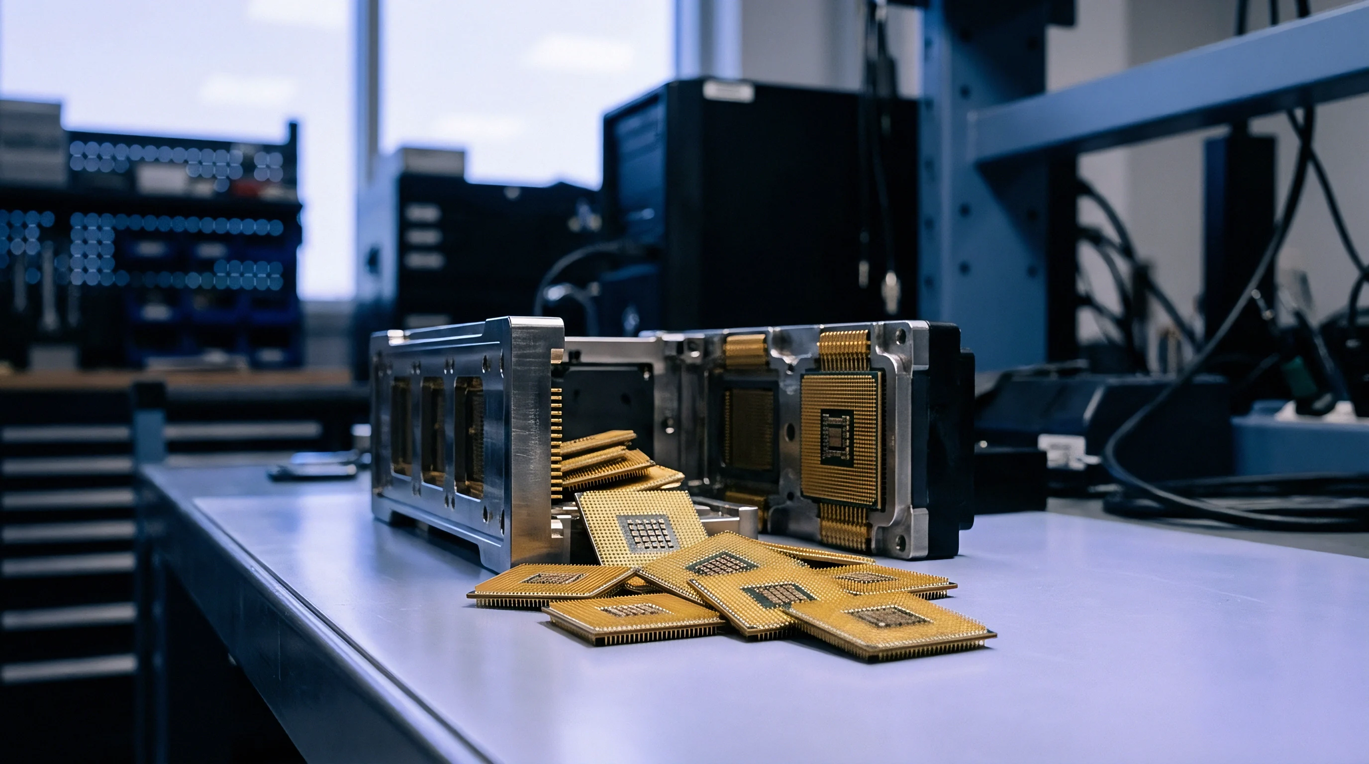
Navigating component shortages requires active engineering management of package substitutions. When primary footprints hit 52-week lead times under supplier allocation controls, pivoting to an alternative package using the identical silicon die can keep production running. This migration requires careful coordination across land-pattern geometry, SMT reflow profiles, and PCB thermal behavior.
Re-spinning a board for an alternative package without complete process qualification risks assembly defects that erase any delivery advantage gained from sourcing the replacement parts.
Die-compatible packages present distinct assembly constraints on the line. Moving from a 0.5mm-pitch QFP to a 0.4mm-pitch WLCSP alters board fabrication requirements: the smaller footprint demands laser-drilled microvias, tighter solder mask registration, and dedicated stencil designs. Placement equipment must hold tighter positional tolerances to handle the finer pitch and lighter component mass without causing bridging or tombstoning during reflow.

Mechanical and Thermal Qualification Parameters
PCB land patterns require adjustments when introducing alternate package outlines. Solder joint fatigue life depends heavily on pad dimensions and stencil aperture geometry. While IPC-7351 standards offer nominal, maximum, and minimum land patterns, emergency substitutions often require customized pads to balance assembly yield against mechanical and thermal strain.
On bottom-terminated components like QFNs, stencil coverage on the exposed center pad must be carefully sectioned to allow flux outgassing and avoid large solder voids that degrade ground and thermal paths.
Reflow profiles must be tuned for every package substitution. Thermal parameters under JEDEC J-STD-020 depend on package thickness and overall mass: compact, thin packages heat faster and reach higher peak body temperatures than bulky molded plastic parts. Running a compact chip-scale part through a reflow profile set for a standard SOIC risks internal delamination, package cracking, or wire bond damage.
Moisture sensitivity levels also vary by package type, demanding updated floor-life monitoring and dry-pack protocols to prevent popcorning during assembly.
- Solder Bridging Failures occur when stencil aperture design fails to account for reduced pitch on alternative package options, leading to adjacent pad shorts during solder reflow.
- Thermal Pad Voiding exceeds 15 percent of total pad area when flux gas evacuation channels are omitted from the solder paste stencil pattern on bottom-terminated parts.
- Package Delamination Defects develop when thin replacement packages pass through reflow profiles intended for high-mass plastic molded components without adjusting thermal ramp rates.
- Joint Fatigue Cracking arises under thermal cycling conditions due to coefficient of thermal expansion mismatch between rigid circuit boards and miniature leadless component packages.
Tray-to-reel format shifts represent another common bottleneck during substitutions. Parts sourced in matrix trays during allocation cycles need tape-and-reel repackaging before high-speed pick-and-place feeders can run them. This transfer adds ESD exposure risks and mechanical lead deformation hazards if handling falls short of ANSI/ESD S20.20 standards.
Procurement schedules must build in repackaging turnaround and incoming inspection times when evaluating alternative package stock.
Package migrations execute cleanly only when land-pattern revisions undergo full solder-joint stress simulation prior to board layout commitment.


Logic
Electrical interface verification is mandatory when changing package variants under allocation pressure. Even when two packages house identical silicon die, structural packaging differences introduce parasitic capacitance, inductance, and resistance that affect signal integrity, bus timing, and EMI performance. Leadframe inductance, bond wire length, and internal package trace geometry vary considerably among DIP, QFP, and WLCSP configurations, altering signal transition times, drive characteristics, and noise margins on digital communication lines.
Bus capacitance constraints set strict limits on signal rise times and maximum interface clocks. The I2C Fast-mode specification caps total bus capacitance at 400pF at 400kHz. Moving to a larger package with greater internal pin capacitance adds load to clock and data lines; an increase of just 3pF per pin across multiple nodes can push rise times beyond the 300ns limit.
Hardware engineers must recalculate pull-up resistor values to maintain sharp transitions without exceeding the driver’s 3mA current sink limit.

Why Does Identical Silicon in New Packaging Trigger Bus Timing Faults?
Package construction dictates the parasitic LCR profile of every lead. Long bond wires in standard molded plastic packages add parasitic inductance up to 5nH per pin, whereas direct solder bumps on chip-scale parts keep inductance under 0.5nH. That reduction alters signal slew rates and can introduce high-frequency ringing.
Output drivers engineered to drive higher package inductances can cause severe ground bounce when mounted in low-inductance packaging, resulting in false triggers on edge-sensitive interrupts or SPI clock lines.
| Package Form Factor | Pin Inductance Range (nH) | Pin Capacitance Range (pF) | Thermal Resistance R_thja (C/W) | Max Recommended Clock Speed |
|---|---|---|---|---|
| Plastic Dual In-Line (PDIP) | 3.5 to 10.0 | 1.5 to 3.0 | 65 to 85 | 12 MHz |
| Small Outline Integrated Circuit (SOIC) | 2.0 to 5.0 | 0.8 to 2.0 | 90 to 110 | 25 MHz |
| Quad Flat No-Lead (QFN) | 0.5 to 1.5 | 0.3 to 0.8 | 35 to 50 | 100 MHz |
| Wafer-Level Chip-Scale (WLCSP) | 0.1 to 0.5 | 0.1 to 0.4 | 40 to 60 | 200 MHz |
Firmware changes are often necessary when swapping package variants. The internal register map may be identical across packages sharing a die, but default pin multiplexing and power-up configurations can change. Some microcontrollers tie configuration pads directly to internal bond wires based on pin count.
A lower-pin-count package may ground certain configuration lines internally, locking out features available on higher-pin variants. Firmware teams must review startup routines to ensure initialization code does not write to unbonded or reassigned pins.
Bus capacitance shifts exceeding 10pF alter signal rise times enough to cause intermittent communication dropouts on Fast-mode I2C lines.
High-speed SPI timing margins require re-validation after any package change. Master-in-slave-out setup and hold times depend on propagation delays through package leads and host controller I/O. Added lead capacitance stretches propagation delays, closing the valid data window at clock speeds above 20MHz. Firmware drivers may need to shift SPI clock phase settings or reduce bus speeds if physical testing shows setup time violations on replacement packages.
Unresolved noise spikes on edge-sensitive clock lines raise the question of whether host-side software filtering can compensate for physical bus ringing without introducing unacceptable processing latency.


Calculus
Working around allocation controls requires direct mathematical modeling of order fulfillment against factory rationing multipliers. Buyers cannot simply issue standard purchase orders; delivery schedules must be structured around vendor allocation equations to capture required unit volume without generating unfulfilled backlog penalties. Modeling historical entitlements, dynamic allocation multipliers, standard packaging increments, and safety stock burn rates allows procurement to build functional supply plans during shortage cycles.
Take an operational scenario where a plant requires 45,000 ICs per quarter to maintain production schedules. The supplier announces allocation and sets an allocation multiplier alpha equal to 0.40 against historical accounts. The customer holds a historical quarterly entitlement B of 30,000 units based on the preceding four-quarter average.
The supplier applies a standard Tape-and-Reel Packaging Quantity Q_reel of 3,000 units per reel and rounds order volumes down to the nearest full reel.

Allocation Fulfillment Arithmetic Walkthrough
The allocation engine calculates the raw unconstrained allocation A_raw from the baseline entitlement equation:
A_raw = alpha B
Applying the scenario values yields:
A_raw = 0.40 30,000 = 12,000 units
The system evaluates packaging reel constraints using the reel division floor function:
Reels_fulfilled = floor(A_raw / Q_reel)
Reels_fulfilled = floor(12,000 / 3,000) = 4 full reels
Actual Delivered Allocation A_delivered equals:
A_delivered = Reels_fulfilled Q_reel = 4 3,000 = 12,000 units
This delivers a baseline deficit D_quarterly against actual quarterly manufacturing demand D_req of 45,000 units:
D_quarterly = D_req – A_delivered = 45,000 – 12,000 = 33,000 units
To cover this 33,000-unit gap, procurement balances three operational levers: qualifying a secondary package variant with an independent baseline entitlement, placing split orders through authorized distribution, and drawing down internal buffer stock.
Assume engineering qualifies an alternative QFN package carrying the identical die. The supplier applies an independent allocation multiplier beta of 0.55 to this QFN line because assembly capacity is less constrained. The buyer holds a secondary quarterly baseline B_secondary of 20,000 units for this part.
The secondary unadjusted allocation calculates to:
A_secondary_raw = beta B_secondary = 0.55 20,000 = 11,000 units
Applying the 3,000-unit reel increment constraint:
Reels_secondary = floor(11,000 / 3,000) = floor(3.666) = 3 full reels
A_secondary_delivered = 3 3,000 = 9,000 units
Summing primary and secondary package allocations gives the total delivered volume A_total:
A_total = A_delivered + A_secondary_delivered = 12,000 + 9,000 = 21,000 units
The remaining quarterly supply deficit drops to:
D_remaining = 45,000 – 21,000 = 24,000 units
To cover the remaining 24,000-unit shortfall across a 12-month allocation horizon, procurement teams use a structured sequence to reconcile supplier allocations with the factory build plan.
- Audit historical purchase orders across all authorized distributor sales branches to compile an aggregate account entitlement baseline figure.
- Calculate the vendor allocation multiplier across each distinct component package part number to identify package margin preferences.
- Submit split purchase orders matching calculated full-reel increments to prevent automated allocation engine rounding cuts.
- Deplete existing internal safety stock buffers at a controlled rate matched exactly to the calculated quarterly supply deficit.
- Adjust host assembly line scheduling to match verified delivered component volume rather than unconfirmed vendor backlog dates.
Supplier contracts carrying non-cancellable non-returnable terms convert unfulfilled allocation balances into binding financial commitments upon schedule confirmation.
Buffer stock planning must factor in shifting lead-time variance during allocation periods. Classical safety stock equations assume a normal Gaussian distribution of supplier lead times. During supply crunches, lead times behave as multi-week step functions instead of normal curves.
Safety stock calculations must shift to deterministic models where safety stock S_safe equals daily burn rate R_burn multiplied by the lead-time extension delta_T in days. Buyers using standard buffer equations risk line stoppages when factory shipments lag behind unconfirmed vendor commit dates.
Standard commercial supply agreements incorporate ISO 9001 quality audit provisions and JEDEC delivery notification standards that mandate formal written notice 30 days prior to applying algorithmic allocation cuts to active purchase orders.


Pact
Commercial framework agreements govern how allocation algorithms handle customer orders during supply crunches. Non-Cancellable Non-Returnable terms are the primary legal mechanism chipmakers use to firm up order books when capacity runs short. Under an NCNR agreement, purchase orders bypass phantom demand filters and gain priority placement in fab production queues.
In exchange, the buyer assumes full financial liability for the volume ordered, forfeiting standard cancellation windows and push-out options.
Take-or-pay structures create significant financial exposure if end-market demand drops unexpectedly. Under these terms, the buyer commits to taking a set volume over a contract window, typically 12 to 24 months. If product demand falls off during that period, the customer must still pay for the contracted units or cover penalty fees matching the supplier’s lost gross margin.
Sourcing managers have to weigh the allocation priority gained under binding commitments against the risk of building excess inventory once the supply crunch eases.

Contractual Allocation Prioritization Models
Capacity Reservation Agreements provide a direct financial path to secure fab allocations during supply crunches. Unlike standard purchase orders, capacity reservation contracts require an upfront, non-refundable fee per wafer start or per thousand packaged parts to lock in dedicated line capacity. Procurement teams weigh these upfront fees against the cost of factory downtime to identify the economic break-even point for paid allocation access.
| Contract Structure Type | Allocation Engine Priority Factor | Downside Cancellation Penalty | Minimum Binding Window | Financial Exposure Horizon |
|---|---|---|---|---|
| Standard Purchase Order | Low (Subject to standard trimming) | Zero penalty outside 30-day window | 30 days lead time | Limited to open order balance |
| Non-Cancellable Non-Returnable (NCNR) | High (Bypasses phantom demand filters) | 100 percent of ordered unit value | 90 to 180 days fixed | Full purchase order line balance |
| Take-or-Pay Capacity Framework | Very High (Direct fab schedule lock) | 70 to 90 percent of contract deficit | 12 to 24 months rolling | Total contractual volume liability |
| Paid Capacity Reservation (CapRes) | Highest (Dedicated wafer reservation) | Forfeiture of upfront reservation fee | 6 to 12 months fixed | Upfront reservation fee plus unit cost |
Evaluating commercial risks requires strict contractual auditing before signing binding allocation agreements during supply crunches.
- Unilateral Schedule Adjustment Rights allow semiconductor vendors to move confirmed delivery dates without financial penalty while holding the buyer to strict NCNR payment terms.
- Volume Slippage Escalation Clauses increase unit pricing automatically if the vendor fails to deliver the contracted baseline volume due to internal fab allocation cuts.
- Package Discontinuation Liabilities force buyers to accept legacy package end-of-life builds under non-returnable terms without providing guaranteed functional replacements.
- Distributor Pass-Through Risk emerges when authorized distributors add margin markups and handling fees to vendor-imposed NCNR agreements without transferring factory allocation rights.
Managing commercial allocation frameworks requires tight alignment between procurement commitments and engineering qualification. Securing allocation priority through binding contracts while qualifying alternate packages on the bench protects factory output across volatile market cycles. Grounding procurement decisions in allocation engine logic, electrical interface constraints, and contractual risk turns component sourcing into a predictable engineering control loop.