Package Configuration
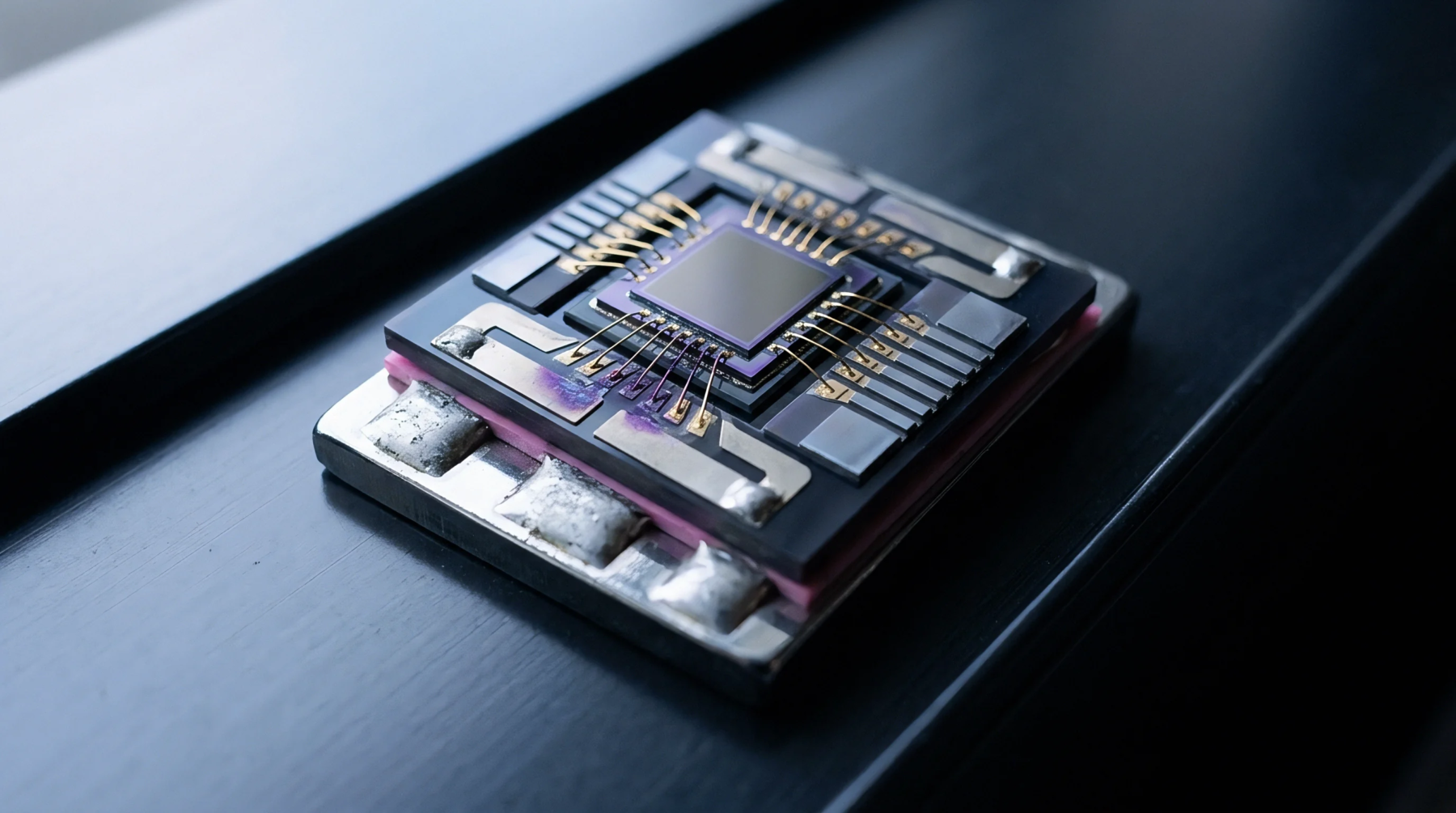
A small outline integrated circuit consists of a semiconductor device mounted within a rectangular plastic body with gull wing leads extending from two parallel sides. This soic structure provides a surface mount alternative to through hole packages for various analog or digital components. The geometry facilitates automatic assembly onto printed circuit boards by allowing leads to sit directly on copper pads.
Manufacturers define the footprint based on lead pitch and body width, creating a standard that governs spatial layout for component placement. The boundary of this physical form stops at the perimeter of the lead pattern, leaving connections to the internal die and wire bonds outside the scope of the geometric specification.
Thermal Resistance
Proper heat dissipation demands careful attention to the contact area between the soic lead frame and the substrate. Thermal energy conducts from the silicon die through the lead frame into the solder joints, which transfers heat toward the board planes. If the power dissipation exceeds the capability of the package design, the die temperature increases until electrical performance degrades or device failure occurs.
Design engineers calculate the junction to ambient resistance to determine whether supplementary cooling or wider copper traces are necessary for operation. Increased power density in smaller body variants forces a trade off where current carrying capacity limits the function of the hardware. The connection quality between the leads and the board determines the stability of the entire thermal path under heavy electrical loads.
Mechanical Tolerance
Standard bodies require precise lead co-planarity to ensure each pin touches the solder paste during the reflow process. A soic package exhibits a variation in vertical lead position, which the assembly technician measures relative to the seating plane. Excessive skew prevents a contact from forming a reliable metallurgical bond, creating an open circuit condition or high resistance path.
The manufacturing facility verifies this alignment using optical inspection systems that scan for displacement from the nominal height. Any deviation beyond the specified limit risks cold solder joints, which appear after the cooling phase of production. Mechanical stresses during board handling or shipping further test the integrity of these joints, making the initial flatness of the component critical for long term reliability.
Calibration Drift
Metrological testing shows that electronic parameters shift when the soic undergoes repeated thermal cycling in the field. This drift originates from the expansion mismatch between the plastic mold compound and the internal lead frame material, which induces mechanical strain on the integrated wire bonds. Technicians calibrate the device at specific reference conditions to account for these shifts, but the adjustment does not remove the underlying physical vulnerability of the architecture.
Interference from high frequency electromagnetic fields also couples into the lead geometry, creating noise that alters the accuracy of sensitive signals. Precision instrumentation confirms that the measured output deviates from the intended transfer function due to these mounting effects. The component accuracy depends on the stability of the mounting conditions provided by the host assembly.