One Die Reaching the Market as Component Module and Probe
Selecting die packaging forms requires matching land pattern mechanical stress, bus wiring distance, and calibration stability against landed unit economics.
Substrate
A bare piezoresistive pressure sensor element measuring 1.8 mm by 1.8 mm by 0.4 mm leaves the fab wafer line with raw bond pads. Downstream packaging transforms this single piece of silicon into five distinct commercial products. The basic wafer-level chip-scale package exposes bare silicon directly to the printed circuit board through solder balls on a 0.4 mm pitch.
When mounted directly on a standard 1.6 mm FR-4 board, structural stresses from the host circuit flow into the silicon lattice. Monocrystalline silicon has a thermal expansion coefficient of 2.6 ppm per degree Celsius, compared to 14 to 17 ppm per degree Celsius for standard FR-4. Temperature swings induce mechanical shear across the interconnect array, warping the sensing element and shifting the zero-point voltage calibration.
The Land Pattern drawing specifies pad geometry and trace routing under bottom-terminated components. Traces routed directly beneath an exposed silicon die create localized height variations in solder mask, producing point-contact mechanical stress during board assembly. A solder mask height variation exceeding 8 µm across the die footprint introduces measureable baseline drift.
Trace geometry proves particularly critical during high-g vibration runs on thin substrate stack-ups.
Die Mechanics and Land Pattern Tolerances
Positioning the raw element inside a molded Land-Grid Array package mitigates direct thermal stress through an intermediate organic substrate. The LGA enclosure measures 3.0 mm by 3.0 mm with a 0.9 mm height profile, containing an internal wire-bonded structure encapsulated by an open-cavity gel ring. The internal substrate absorbs thermal expansion mismatches between the primary circuit board and the silicon wafer element.
Land pattern recommendations according to IPC-7351B specify copper pad dimensions of 0.35 mm by 0.45 mm for perimeter pads on a 0.65 mm pitch. Tolerances on land dimensions require tighter control than standard surface mount passives. A copper etch variance of plus or minus 15 µm alters the surface tension balance during reflow, pulling the component off-center by up to 35 µm.
Off-center placement disrupts the gel seal geometry when mating an external environmental port gasket.
| Packaging Form Factor | Physical Footprint (mm) | Height Profile (mm) | Package Thermal CTE (ppm/°C) | Moisture Sensitivity Level |
|---|---|---|---|---|
| Wafer-Level Chip-Scale Package (WLCSP) | 1.80 × 1.80 (±0.02) | 0.40 (±0.03) | 2.6 (Silicon native) | MSL 1 |
| Land-Grid Array (LGA) Molded | 3.00 × 3.00 (±0.10) | 0.90 (±0.08) | 6.5 to 8.5 (Organic Substrate) | MSL 3 |
| Board-Level Module (PCB Substrate) | 12.00 × 18.00 (±0.15) | 3.20 (±0.20) | 14.0 to 16.0 (FR-4 Rigid) | MSL 3 (SMD Parts) |
| Cabled Industrial Probe | 12.00 Diameter (±0.05) | 65.00 Length (±0.50) | 12.0 (316L Stainless Steel) | IP68 / NEMA 6P |
| Housed Heavy Industrial Transmitter | 85.00 × 110.00 (±1.00) | 65.00 Profile (±1.00) | 23.0 (Aluminum Die-Cast) | IP67 / NEMA 4X |
Die attach adhesives inside molded components determine mechanical stress transmission from the package base to the piezoresistive bridge. Soft silicone adhesives featuring a low Young’s modulus below 5 MPa isolate the wafer from substrate strain. Hard epoxy adhesives with a modulus exceeding 3000 MPa transmit substrate deflection straight to the sensing element.
Selection of the mounting material alters thermal hysteresis from 0.05 percent of full scale output to 0.45 percent over a thermal span of -40 °C to 125 °C.
A board thickness variance of 0.4 mm increases die piezoresistive zero-point offset drift by 1.8 Pascal per degree Celsius under thermal cycling between -40 °C and 85 °C.
Board Flexure and Stress Coupling
Bending forces applied to the host circuit assembly translate into mechanical deformation of the sensor die housing. Mounting holes located closer than 8.0 mm to the component perimeter transfer screw torque directly through copper ground layers into solder joints. Board deflection of 1.0 mm per 100 mm span shifts the uncompensated zero-point voltage by up to 2.4 mV on a 3.3 V supply, as mechanical tension feeds directly into the silicon.
Mechanical stress coupling follows predictable paths across the assembly layout:
- Asymmetrical Copper Distribution shifts board strain unevenly across the package perimeter during reflow cooling cycles.
- Heavy Component Placement adjacent to the sensitive element causes mechanical sagging and local thermal gradients across the ground plane.
- Conformal Coating Accumulation under the package body introduces uneven lifting forces during solvent evaporation and curing.
- Connector Insertion Shear creates transient physical displacement that permanently shifts baseline bridge resistance values.
Redesigning the board stack-up mitigates mechanical deformation. Placing copper keep-out zones on inner layers directly beneath the sensor package isolates the die from internal plane tension. Symmetrical routing of top-layer trace connections balances physical forces acting on individual perimeter solder pads.
Mounting a bare LGA footprint directly adjacent to a rigid structural mounting post resulted in a zero-point re-calibration charge of 14,000 dollars.


Joint
Surface mount assembly of small-footprint sensor packages depends on tight control of solder paste deposition and reflow thermal profiles. IPC-A-610 standards govern acceptable reflow joint formation for bottom-terminated components like LGAs and QFNs. Lead-free solder alloys containing SAC305 (96.5% Tin, 3.0% Silver, 0.5% Copper) feature a liquidus temperature of 217 °C, requiring peak reflow temperatures between 235 °C and 250 °C. Exceeding peak reflow temperature limits damages internal wire bonds and degrades open-cavity gel sealants.
Solder paste stencil aperture design governs solder volume under LGA perimeter pads. Apertures cut at a 1:1 ratio relative to board lands output excess solder volume, generating liquid solder bridges beneath the package body. A 10 percent reduction in stencil aperture area using laser-cut nickel-coated stencils yields a controlled solder volume of 0.0035 mm³ per pad.
Solder voids beneath thermal pads or mechanical grounds destabilize thermal dissipation paths and introduce local mechanical tilt during joint solidification.

Reflow Profiles and Thermal CTE Mismatch
Thermal ramp rates during reflow heating influence internal package stresses. JEDEC J-STD-020E defines maximum ramp-up rates of 3 °C per second to prevent thermal shock in sensitive moisture-exposed components. Rapid heating drives moisture trapped in organic substrates to expand, causing internal package delamination or popcorning.
Moisture Sensitivity Level 3 (MSL 3) components require baking at 125 °C for 24 hours prior to surface mount assembly if exposed to ambient factory conditions exceeding 30 °C and 60 percent relative humidity for longer than 168 hours.
Compliance with JEDEC J-STD-020E mandates floor life tracking once moisture barrier bags open, preventing delamination failures during lead-free reflow at 260 °C peak temperature.
Thermal cycling tests performed in accordance with JESD22-A104 evaluate long-term solder joint integrity under stress. Subjecting assemblies to 1,000 cycles between -40 °C and 125 °C reveals creep rupture mechanisms in perimeter solder connections. Thermal expansion mismatches between the organic package substrate (8 ppm/°C) and the FR-4 mainboard (16 ppm/°C) concentrate shear strain inside outer corner joints.
Micro-cracks initiate at the outer intermetallic compound layer, propagating inward until line continuity breaks.

Voiding Ratio and Stencil Aperture Ratios
X-ray inspection measures solder voiding percentage beneath bottom pads. Standard IPC-7093 Class 2 guidelines permit up to 25 percent total voiding area under central thermal grounding pads. Precision sensor applications require voiding rates below 10 percent to guarantee physical stability and mechanical zero-point repeatability.
High void content creates asymmetric mechanical stiffness across the package foundation, causing the die to tilt relative to the board plane.
Modifying stencil geometry from solid rectangular apertures to a cross-hatched grid array reduces gas trapping during flux volatile outgassing. Grid apertures featuring 0.15 mm web gaps provide escape channels for flux vapor before the solder alloy reaches its liquidus phase. Solder ball formation outside designated land areas occurs when reflow pre-heat slopes drop below 1 °C per second, allowing flux to slump and carry alloy particles onto solder mask regions.
Field failure analysis of returned assembly lots showed perimeter joint lifting following environmental thermal cycling. Post-assembly board washing solvents cause micro-fractures in solder joints by inducing localized chemical corrosion under package corners.


Signaling
The host system reads data from the sensor element through digital or analog interfaces adapted to each packaging form factor. Bare WLCSP and molded LGA variants export raw digital lines such as I2C or SPI direct to local host microcontrollers. Board-level modules combine the sensor die with an onboard signal conditioning application-specific integrated circuit (ASIC), offering pre-calibrated I2C, SPI, or high-speed UART outputs over castellated edge pins.
Cabled industrial probes transform internal digital frames into differential protocols like RS-485 Modbus RTU or 4-20 mA analog current loops for long-distance industrial wiring.
Choice of interface determines physical wiring distance, noise immunity, host driver complexity, and power dissipation. The basic I2C bus operates over two bidirectionally pulled-up lines (SDA and SCL) limited by standard specifications to a total bus capacitance of 400 pF in Fast-mode (400 kHz) or 550 pF in Fast-mode Plus (1 MHz). Routing I2C signals through long cabled interconnects increases trace capacitance beyond allowed thresholds, degrading clock rise times and causing bit corruption.

Bus Line Capacitance and Driver Timings
Calculating pull-up resistor values balances rise time limits against low-level output current drive capabilities. Maximum rise time for Fast-mode I2C signals equals 300 ns. Given a total bus capacitance of 150 pF on a 0.5-meter internal module ribbon cable, minimum pull-up resistance equals 1.2 kΩ for a 3.3 V supply voltage, drawing 2.75 mA during output low state drive cycles.
Lower resistor values decrease rise time but increase overall operating current, raising package self-heating and introducing local thermal offset errors into sensor bridge readings.
| Interface Protocol | Physical Layer Standard | Maximum Distance (m) | Bus Capacitance Cap (pF) | Driver Firmware Weeks |
|---|---|---|---|---|
| I2C Fast-Mode Plus | Open-Drain CMOS (3.3V) | 0.50 | 550 | 2.0 |
| SPI Mode 0/3 | Push-Pull CMOS (3.3V) | 0.15 | 100 | 1.5 |
| RS-485 Modbus RTU | Differential EIA-485 | 1200.00 | Unbounded (Z0 = 120Ω) | 4.0 |
| 4-20 mA Loop | Current Loop Analog | 3000.00 | Unbounded (Loop Res) | 1.0 |
| 0-10 V Analog | Voltage Mode Analog | 10.00 | 1000 | 0.5 |
High-speed SPI interfaces run push-pull driver outputs capable of reaching clock speeds up to 20 MHz. SPI lines require termination resistors when trace lengths exceed one-tenth of the signal propagation wavelength on the board. A 50-ohm series termination resistor placed next to the host SPI clock pad suppresses signal reflection undershoot and overshoot, preserving timing margins across setup time (tSU = 5 ns) and hold time (tHD = 5 ns) windows defined in ASIC registers.
Bringing up an integrated digital sensor module requires a systematic electrical and firmware verification sequence to ensure robust operation under harsh EMI conditions:
- Apply target VDD supply voltage with a ramp rate under 10 mV/µs to verify internal Power-On Reset (POR) circuit triggering.
- Probe the SDA and SCL lines with an oscilloscope to confirm idle high levels match VDD within a 5 percent tolerance margin.
- Issue an I2C bus reset sequence consisting of nine clock pulses followed by a STOP condition to clear locked slave bus states.
- Read the internal WHO_AM_I register (0x0F) and verify returned static device identification byte matches product documentation.
- Write zero-point calibration trim coefficients into volatile configuration registers prior to initiating sensor sampling commands.
- Measure data ready (DRDY) interrupt pin response pulse width to confirm internal measurement cycle completion timing.
Modbus RTU implementation over RS-485 requires hardware transceiver integration inside the probe housing, adding firmware development time. Transceivers such as MAX3485 operate over a wide common-mode voltage range (-7 V to +12 V), isolating sensitive silicon ASIC lines from high-voltage transient spikes induced on industrial wiring runs. Differential signaling handles transmission over distances up to 1,200 meters using twisted-pair shielded cabling terminated with 120-ohm matching resistors at physical bus ends.

Transceiver Integration and Protocol Bridging
Translating internal digital signals into analog current loop outputs requires an onboard digital-to-analog converter (DAC) coupled to a precision current regulator. The 4-20 mA current loop standard maps zero-scale sensor readings to 4.0 mA and full-scale readings to 20.0 mA. The lower 4.0 mA floor supplies operating power to internal sensor electronics and microcontrollers, leaving 3.5 mA maximum current budget for active silicon operation.
Power supply rejection ratio (PSRR) specifications inside current loop transmitters must exceed 80 dB to suppress power line ripple from reaching internal analog-to-digital converter (ADC) reference nodes.
Analog voltage outputs (0 to 10 V) require high-side operational amplifier drivers powered from an elevated 24 V industrial supply rail. Amplifiers must drive capacitive loads up to 10 nF without initiating parasitic oscillations. Trace layout between the internal sensor ASIC and the output stage buffer requires physical shielding using copper guard rings to prevent external electrical field coupling from corrupting analog measurement channels.
Bus stress testing over forty meters of shielded twisted pair highlights ongoing debate between hardware engineers and firmware developers over whether active bus pull-up accelerators or physical bus isolators should be mandatory when extended cabled sensor probes operate in high-noise industrial motor environments where ground potential shifts exceed two volts.


Gasket
Converting a bare module into a cabled industrial probe or housed transmitter requires structural encapsulation and environmental sealing. Polyurethane, silicone, and epoxy potting compounds encapsulate internal electronics, shielding them against liquid ingress, corrosive gases, and mechanical vibration. Selection of potting material determines mechanical stress transfer to the internal die element, operating temperature boundaries, and moisture vapor transmission rates.
Physical potting curing dynamics introduce volumetric shrinkage during polymerization. Epoxy potting materials exhibit shrinkage rates between 1.0 and 3.0 percent by volume during heat curing. Curing shrinkage exerts compressive forces exceeding 15 MPa on package walls, squeezing open-cavity Gel ports and displacing internal gel fills.
Encapsulation strain distorts internal piezoresistive element spacing, inducing permanent zero-point calibration shifts up to 3.5 percent of full-scale measurement range.

Potting Encapsulation Stress and Offset Shift
Two-component soft silicone gel encapsulation materials feature low volumetric shrinkage (under 0.1 percent) and low Shore hardness (Shore A 10 to 30). Soft silicone cushions the sensitive silicon die from mechanical deformation while providing electrical insulation up to 18 kV/mm. Silicone materials allow moisture vapor migration over time.
Moisture vapor penetrating the gel barrier condenses on internal metal bond wires, promoting electrochemical migration and dendrite growth under continuous DC bias voltage exposure.
| Encapsulation Compound | Shore Hardness | Curing Shrinkage (%) | Thermal Conductivity (W/m·K) | Moisture Transmission Rate |
|---|---|---|---|---|
| Addition-Cure Soft Silicone Gel | Shore A 15 | 0.05 | 0.25 | High (15 to 25 g/m²·day) |
| Semi-Rigid Polyurethane | Shore D 50 | 0.80 | 0.45 | Moderate (3 to 8 g/m²·day) |
| Filled Structural Epoxy | Shore D 85 | 1.50 | 1.10 | Low (< 1 g/m²·day) |
| Fluorosilicone Gel | Shore A 30 | 0.10 | 0.30 | Low (Fuel & Solvent Resistant) |
Rigid epoxy compounds filled with silica particles achieve thermal conductivity values of 1.1 W/m·K, improving heat dissipation from internal power regulation circuits. High thermal conductivity minimizes internal temperature gradients across the sensing bridge, though epoxy’s high mechanical stiffness transmits external casing flexure straight to the internal circuit board. Standard design practices mandate multi-layer encapsulation, applying a soft silicone buffer layer over the sensor element prior to filling the main housing cavity with structural epoxy compound.
Soft silicone potting buffers mechanical strain on exposed silicon while hard epoxy potting transmits enclosure wall deformation directly into the sensing diaphragm.

Media Compatibility and Ingress Barrier Mechanicals
Probes operating in corrosive liquid or high-pressure gas streams require fluid isolation barriers. Stainless steel 316L diaphragms measuring 0.05 mm in thickness isolate the internal sensor die from direct fluid contact. Synthetic oil (such as silicone oil DC200) fills the internal cavity between the isolating diaphragm and the silicon element, transmitting external pressure changes hydrostatically without mechanical loss.
Oil fill volume control requires high precision. An oil fill volume tolerance of plus or minus 0.002 cm³ alters thermal expansion expansion-driven offset errors by 0.12 kPa per degree Celsius.
Sealing external casing joints relies on elastomeric O-rings rated for IP68 environmental protection. Fluorocarbon (FKM) O-rings offer chemical resistance to fuels and solvents but exhibit compression set degradation at temperatures below -20 °C. Ethylene Propylene Diene Monomer (EPDM) O-rings handle low temperatures down to -40 °C but fail rapidly when exposed to petroleum-based lubricants. O-ring groove dimensions according to ISO 3601-2 specify a squeeze ratio between 15 and 25 percent to ensure positive fluid sealing without over-stressing the outer enclosure material during high-pressure immersion cycles.
Long-term immersion under water column pressure causes elastomeric seal compression set failure when mechanical deformation exceeds limits over time.


Qualification
Validating performance across packaging variants requires testing routines that verify register map integrity, thermal calibration stability, and mechanical durability. Semiconductor fabs introduce minor layout adjustments during wafer manufacturing steps, yielding subtle die stepping revisions. While basic sensing functionality remains constant, internal register addresses, factory calibration coefficient scaling factors, or power-on default register values can alter between silicon mask revisions.
Automated test fixtures run register verification sweeps on incoming component lots. Firmware written for Rev A die stepping fails or reads corrupt data when deployed on Rev B silicon if register maps shift without manufacturer notification. Ensuring firmware driver compatibility across five die stepping revisions requires verifying device identification bytes during host software initialization to prevent downstream data corruption.

Silicon Revisions and Register Drift Verification
Factory calibration coefficients stored inside onboard non-volatile memory (EEPROM or OTP memory) compensate for raw piezoresistive bridge non-linearity and temperature sensitivity. Silicon die integration into secondary packages alters raw bridge response characteristics. Packaging stress shifts the zero-point voltage and alters sensitivity coefficients over temperature.
A module manufacturer must execute full secondary thermal calibration across the operating temperature envelope (-40 °C to 85 °C) to generate updated polynomial compensation constants.
Unannounced internal register map updates across silicon die revisions halt host automated bring-up until firmware routines match the active silicon revision code.
Testing procedures measure offset stability, span repeatability, and response time across environmental stress exposures. Reliability qualification follows AEC-Q100 or IEC 60740 standards depending on target automotive or industrial deployment sectors. Temperature-Humidity-Bias (THB) testing exposes components to 85 °C and 85 percent relative humidity for 1,000 hours under operational electrical bias, exposing internal corrosion paths and passive leakage pathways.
Calibration Retention across Form Factor Transitions
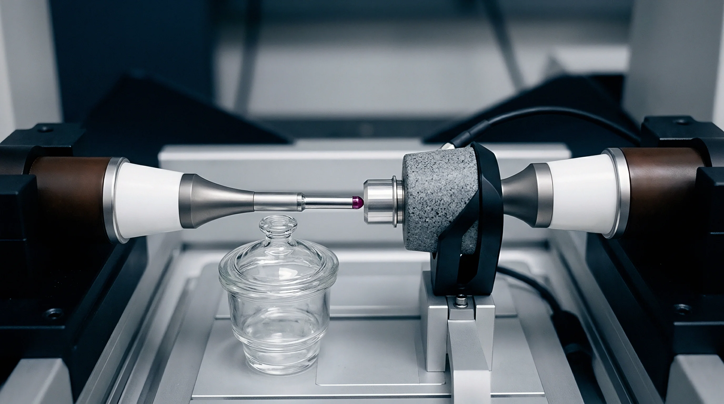
Long-term calibration retention quantifies zero-point drift rates over product operating lifespans. Unpackaged bare die components exhibit low long-term drift under clean dry storage conditions. Enclosed modules and cabled probes suffer drift induced by material outgassing, stress relaxation in potting compounds, and mechanical creep in solder joint arrays.
Drift specifications define maximum allowable baseline shift, typically expressed as plus or minus 0.1 percent of full-scale output per year.
Calibration retention data collected across package variants highlights the impact of physical encapsulation on operational drift rates:
- Bare Silicon Element shows nominal zero-drift under clean hermetic conditions (< 0.02% FSO/year).
- Molded LGA Package exhibits baseline drift driven by organic substrate moisture absorption (0.05% FSO/year).
- Potting Encapsulated Probe suffers stress relaxation drift from surrounding polymer curing networks (0.18% FSO/year).
- Welded Stainless Probe achieves high stability via isolated oil fill mechanical decoupling (0.03% FSO/year).
Verification protocols mandate sample size testing to establish statistical process control capability indices (Cpk). A process capability index exceeding 1.33 confirms that manufacturing variations fall within specified customer tolerance bands across all production lots.
According to section 4.2 of the master supply agreement, any alteration to silicon mask geometry, packaging material composition, or internal assembly location requires formal written customer change notifications six calendar months prior to volume production shipment.


Logistics
Moving one silicon sensor die into five market variants involves substantial differences in unit pricing, minimum order quantities (MOQ), packaging delivery streams, and non-recurring engineering (NRE) investment. A single silicon die produced on an 8-inch wafer yields approximately 15,000 functional dice at a raw wafer manufacturing cost below 1.20 dollars per piece. Packaging, testing, calibrating, and housing that single die scales the unit price by a factor of nearly one hundred across the product hierarchy.
Low-volume industrial applications cannot absorb the high NRE tooling costs and automation setup expenses required to design and assemble custom surface-mount board modules or sealed cabled probes. Sourcing higher-level variants off-the-shelf shifts manufacturing complexity to specialized assembly suppliers, trading higher bill of materials (BOM) cost for lower upfront engineering investment.
Five-Variant Unit Cost Breakdown
Commercial structures vary across packaging levels. Bare die and WLCSP components ship in wafer tape or tape-and-reel quantities of 5,000 units, targeting automated high-speed surface-mount assembly lines. Molded LGA packages ship in standard tape-and-reel reels of 1,000 to 3,000 units.
Board-level modules ship in cut-tape or anti-static trays with lower minimum order limits (100 units). Cabled probes and housed transmitters ship as individually boxed, serialized units with zero MOQ constraints but substantially higher per-unit landed costs.
| Variant Form Factor | Unit Cost @ 1k (USD) | Unit Cost @ 50k (USD) | Minimum Order Qty (MOQ) | Tooling / NRE Cost (USD) |
|---|---|---|---|---|
| Bare WLCSP Die | 1.85 | 0.72 | 5,000 | 0 |
| Molded LGA Component | 3.80 | 1.45 | 1,000 | 0 |
| Board-Level Module | 9.50 | 4.20 | 100 | 2,500 (Custom PCB) |
| Cabled Industrial Probe | 34.00 | 16.80 | 10 | 12,000 (Injection Mold/Machining) |
| Housed Heavy Transmitter | 115.00 | 58.00 | 1 | 35,000 (Enclosure Tooling) |
Developing a custom cabled probe housing requires investment in machining fixtures, injection molding tooling for cable relief grommets, and automated potting dispensing setups. Total initial NRE expenditure easily exceeds 15,000 dollars for specialized mechanical assemblies.

Make-or-Buy Break-Even Volume Analysis
The financial break-even point between buying an integrated cabled probe versus manufacturing the probe assembly in-house depends on production volume and internal assembly line yields. Shifting from cabled probes to integrated modules at twenty thousand annual units yields a net saving of 14 percent. Calculating total landed cost requires factoring in component purchase price, assembly line labor hours, potting scrap rates, calibration equipment depreciation, and yield losses during final testing.
At annual production volumes below 2,500 units, purchasing pre-calibrated cabled industrial probes at 34.00 dollars per unit avoids capital expenditure for thermal calibration chambers and pressure testing rigs. When production volume rises above 15,000 units annually, the amortized cost of custom internal module assembly drops total unit cost to 18.50 dollars, justifying internal manufacturing line establishment.
Freight and logistics packaging selection influences delivered costs. WLCSP and LGA parts ship in light moisture-barrier bags with negligible freight overhead per component. Housed industrial transmitters weigh up to 850 grams each, adding substantial international air freight and import tariff duties to the final delivered bill of materials cost.
Sourcing decisions balance component land patterns, bus integration effort, manufacturing yield risks, and volume pricing matrices to select the precise package variant required for a given product operational lifespan.