Wafer Level Packaging Thermomechanical Stress Compensation in High Gradient Precision Bandgap Layouts
WLCSP packaging induces mechanical stress gradients that shift bandgap references, requiring rotated common-centroid layouts and active digital trim.

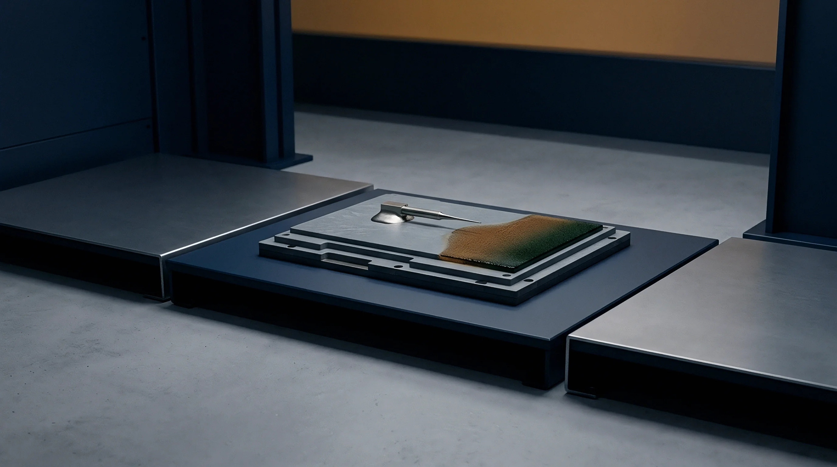
Deformation
Mechanical force alters bandgap reference output through piezoresistive and piezojunction shifts in silicon. When a wafer-level chip-scale package (WLCSP) solders directly to an FR4 printed circuit board, the coefficient of thermal expansion mismatch between silicon (2.6 ppm/K) and the board laminate (14 to 17 ppm/K) generates severe mechanical stress. Solder reflow at 260 degrees Celsius freezes baseline strain into the assembly during cool-down.
Board flexure, thermal cycling, and localized dissipation convert into normal and shear strains across the active die surface. These mechanical loads reach magnitudes from 50 MPa to over 250 MPa near die corners and ball perimeters.
Bipolar junction transistors form the core of bandgap reference architectures. The base-emitter voltage depends directly on the bandgap energy and the saturation current. Compressive stress alters the energy band structure of silicon, lifting conduction band degeneracies and modifying the effective density of states.
Tensile stress shifts the valence band sub-bands. These bandgap modifications change the intrinsic carrier concentration, driving shifts in the base-emitter voltage at fixed collector currents. Concurrently, stress alters majority and minority carrier mobility through piezoresistive coupling, modulating collector current density across matched pairs.
A 100 MPa in-plane normal stress delta shifts base-emitter potential by approximately 0.7 millivolts in standard (100) silicon substrates.
Precision references rely on proportional-to-absolute-temperature (PTAT) and complementary-to-absolute-temperature (CTAT) voltage summation. Thermal gradients across the die induce differential mechanical strain fields. When thermal dissymmetry combines with structural stress gradients, matched bipolar transistor pairs experience asymmetric mechanical bias.
A difference in stress between the unit core transistor and the ratioed peripheral array introduces an uncompensated delta in base-emitter voltage. The output voltage drifts from its nominal calibrated value, degrading long-term stability and elevating temperature coefficients past target system tolerances.
Die thinning accelerates this physical vulnerability. Standard WLCSP grinding targets wafer thicknesses between 200 and 400 micrometers to fit low-profile board constraints. Thinner silicon exhibits lower structural stiffness, transferring a higher proportion of board-level solder joint strain directly into the active epitaxial layer.
Packaging engineers counter this transmission through specialized redistribution layers, mechanical isolation trenches, and layout orientations positioned along stress-neutral crystal axes.
Ignoring packaging-induced stress gradients during layout generation causes factory trim calibrations to fail after surface mount board assembly, forcing expensive printed circuit rework cycles.

Bump
Solder interconnect geometry governs the spatial profile of shear force transfer into the underlying die. Wafer-level packages place SAC305 or SAC405 alloy spheres on under-bump metallization pads arrayed across the active circuitry. Each solder ball acts as a rigid point anchor during thermal transitions.
Thermal displacement expands outward from the die neutral point, concentrating peak strain energy at corner interconnects. The distance from the neutral point dictates the mechanical strain magnitude experienced by nearby transistors.
Copper pillar interconnects alter this mechanical coupling. A solid electroplated copper column with a lead-free solder cap provides a defined standoff height with tight dimensional control. Copper possesses an elastic modulus of approximately 120 GPa, exceeding the compliant modulus of standard solder alloys.
This stiffness elevates localized shear stress beneath the under-bump metallization while restricting out-of-plane board warpage. Die passivation layers, often comprised of silicon nitride beneath polyimide or polybenzoxazole buffers, absorb these concentrated edge stresses.
| Material Layer | Elastic Modulus (GPa) | Thermal Expansion (ppm/K) | Poisson Ratio | Yield Strength (MPa) |
|---|---|---|---|---|
| Silicon Substrate | 130 to 169 | 2.6 | 0.28 | 7000 |
| Polyimide Buffer | 3.0 to 5.0 | 35.0 | 0.34 | 140 |
| Copper Pillar | 115 to 128 | 16.5 | 0.34 | 220 |
| SAC305 Solder | 40 to 50 | 21.0 | 0.36 | 35 |
| FR4 PCB Core | 18 to 24 | 14.0 to 17.0 | 0.15 | 180 |
Redistribution layer routing introduces asymmetric mechanical fields across the die surface. Thick copper traces on the front side create localized tensile pulling forces as temperatures drop from curing thresholds. Thicker dielectric polymer layers damp these forces.
Applying a 5 to 10 micrometer polyimide redistribution buffer isolates the silicon surface from the direct shear profile of the copper trace stack. Layout drafts require strict trace symmetry above sensitive analog circuitry.
- Interconnect array pitch sets the base spatial clearance available for isolation rings and dictates local stress concentration factors around each pad.
- Under-bump metallization diameter controls the solder wetting perimeter and fixes the mechanical anchor area on the top passivation layer.
- Polymer passivation thickness establishes the elastic compliance between rigid copper redistribution lines and fragile active silicon structures.
- Standoff height consistency prevents uneven board tilt that introduces directional shear planes across the underlying reference layout.
Foundry representatives regularly assert that standard polyimide buffering layers absorb all packaging stresses without requiring circuit layout adjustments.

Geometry
Layout topology provides the primary defense against packaging-induced thermal and mechanical gradients. Placing sensitive bandgap core transistors along specific crystallographic directions minimizes piezoresistive sensitivity. For standard (100) p-type silicon wafers, the and axes exhibit lower longitudinal and transverse piezoresistive coefficients for NPN and PNP devices compared to the standard cleavage planes.
Rotating the core bandgap transistor matrix 45 degrees relative to the die edges reduces mechanical sensitivity to external package stress.
Cross-quad common-centroid configurations cancel linear gradients across spatial axes. When a thermal or strain gradient propagates across a transistor array, a simple side-by-side pair experiences asymmetric biasing. Distributing the core pair into four, eight, or sixteen cross-coupled unit devices averages linear gradients to zero at the geometric centroid.
High-order non-linear stress gradients from nearby solder balls resist simple centroid compensation, demanding higher-order circular or matrix symmetry.
| Layout Topology | Linear Gradient Cancellation | Circular Stress Rejection | Silicon Area Overhead | Target Precision (ppm/K) |
|---|---|---|---|---|
| Standard Differential Pair | Poor | None | 1.0x (Baseline) | 50 to 100 |
| Cross-Quad Common-Centroid | High | Moderate | 1.8x to 2.2x | 10 to 25 |
| Hexadecimal Cross-Matrix | High | High | 3.5x to 4.5x | 3 to 8 |
| Concentric Radial Quad | Moderate | Complete | 2.8x to 3.2x | 5 to 12 |
Dummy devices maintain uniform structural boundary conditions around active cores. Edge transistors in an unshielded array encounter asymmetric lithographic etching, shallow trench isolation stress, and localized oxide dishing. Surrounding the active common-centroid core with dummy transistor rings balances the mechanical boundary conditions.
These dummy rings absorb boundary shear generated by adjacent metallization stacks.
Placing active reference cores within the central thirty percent of die area isolates them from steep edge-effect stress fields.
Deep trench isolation rings provide physical mechanical decoupling. Etching narrow trenches around the core reference cell and refilling them with compliant dielectric materials interrupts the lateral propagation of shear waves. Layout engineers position the sensitive core at the die geometric center, maximizing the distance to the outer edges and packaging corners where board warpage forces concentrate.
Symmetric placement around the die neutral point maintains reference balance under uniform thermal expansions.

Correction
Digital compensation schemes augment physical layout isolation to nullify residual packaging drift. On-chip piezoresistive stress sensors, fabricated using matched p-type and n-type diffusion resistor bridges, measure localized stress components in real time. These sensor bridges output differential voltages proportional to the sum and difference of in-plane normal stresses.
An auxiliary analog-to-digital converter digitizes this stress reading alongside die temperature data.
The host system or an embedded microcontroller applies polynomial correction coefficients stored in non-volatile memory. Factory wafer probing captures baseline un-stressed voltage characteristics. Post-assembly testing records the post-packaging offset.
The difference between these states populates the calibration matrix. When thermal or mechanical loads change during field operation, the digital core recalculates trimming currents, steering digital-to-analog converter trim networks connected to the bandgap summing nodes.
- Piezoresistive sensor readout captures in-plane mechanical stress tensors via a dedicated low-noise differential amplifier channel.
- Temperature sensor conversion measures the absolute silicon core temperature to decouple thermal shifts from pure mechanical strain.
- Matrix polynomial evaluation computes the required correction word using pre-programmed coefficients via an embedded state machine.
- Current-steering trim execution applies binary-weighted currents into the PTAT and CTAT summing junctions to restore the target bandgap voltage.
Digital trimming interfaces operate over standard I2C or SPI serial buses. Fast mode I2C runs at 400 kHz with standard 7-bit addressing, while SPI interfaces accommodate clock rates up to 20 MHz for rapid sensor telemetry streaming. Dedicated register maps store raw stress data, temperature codes, and trim values.
System designers access these registers during board-level calibration routines to verify that mechanical shifts stay within compensation bounds.
JEDEC standard JESD22-A104 thermal cycling conditions define the endurance boundary for active stress-trim registers.
Under section 4.3 of procurement standard IPC-9701, thermal cycling qualification mandates uninterrupted solder joint integrity without register corruption across 1000 thermal cycles between -40 and +125 degrees Celsius.

Procurement
Selecting package variants requires balancing board area constraints against downstream calibration expenses. A single precision bandgap core reaches the market across multiple form factors: bare wafer-level chip-scale packages, molded quad-flat no-leads (QFN) packages, small outline integrated circuit (SOIC) enclosures, and hermetic ceramic packages. Each form factor introduces distinct thermomechanical boundaries that dictate production test yield and board integration effort.
| Package Form | Footprint Area (mm²) | Assembly SMT Yield | Unit Cost Delta | Post-SMT Drift (ppm) |
|---|---|---|---|---|
| 4-Ball WLCSP (0.4 mm pitch) | 0.64 to 1.00 | 98.2% to 99.1% | 1.0x (Baseline) | 150 to 300 |
| 6-Lead DFN (2×2 mm) | 4.00 | 99.6% to 99.8% | 1.3x to 1.5x | 60 to 120 |
| 8-Lead SOIC | 24.50 | 99.9% to 99.95% | 1.8x to 2.2x | 20 to 50 |
| 8-Lead Hermetic Ceramic | 35.00 | 99.95% | 8.0x to 12.0x | 5 to 15 |
WLCSP options provide the smallest physical area and lowest initial component price. This form factor shifts mechanical compliance challenges directly to surface mount assembly lines. Board designers must evaluate underfill dispensing costs against solder joint fatigue limits.
Applying capillary underfill stabilizes solder balls against shear fatigue. Underfill curing generates localized compressive shrinkage that introduces additional offset shifts into the reference core.
Molded plastic packages incorporate compliant copper leadframes and epoxy mold compounds. The mold compound isolates the silicon from direct board flexure while introducing hygroscopic expansion risks. Moisture absorption swells the epoxy matrix, producing humidity-dependent reference drift.
Sourcing teams analyze these trade-offs against project volume requirements, field environmental profiles, and end-of-line calibration capabilities.
The remaining question is whether sub-ppm bandgap precision can survive lead-free board reflow without on-chip active strain sensing networks.