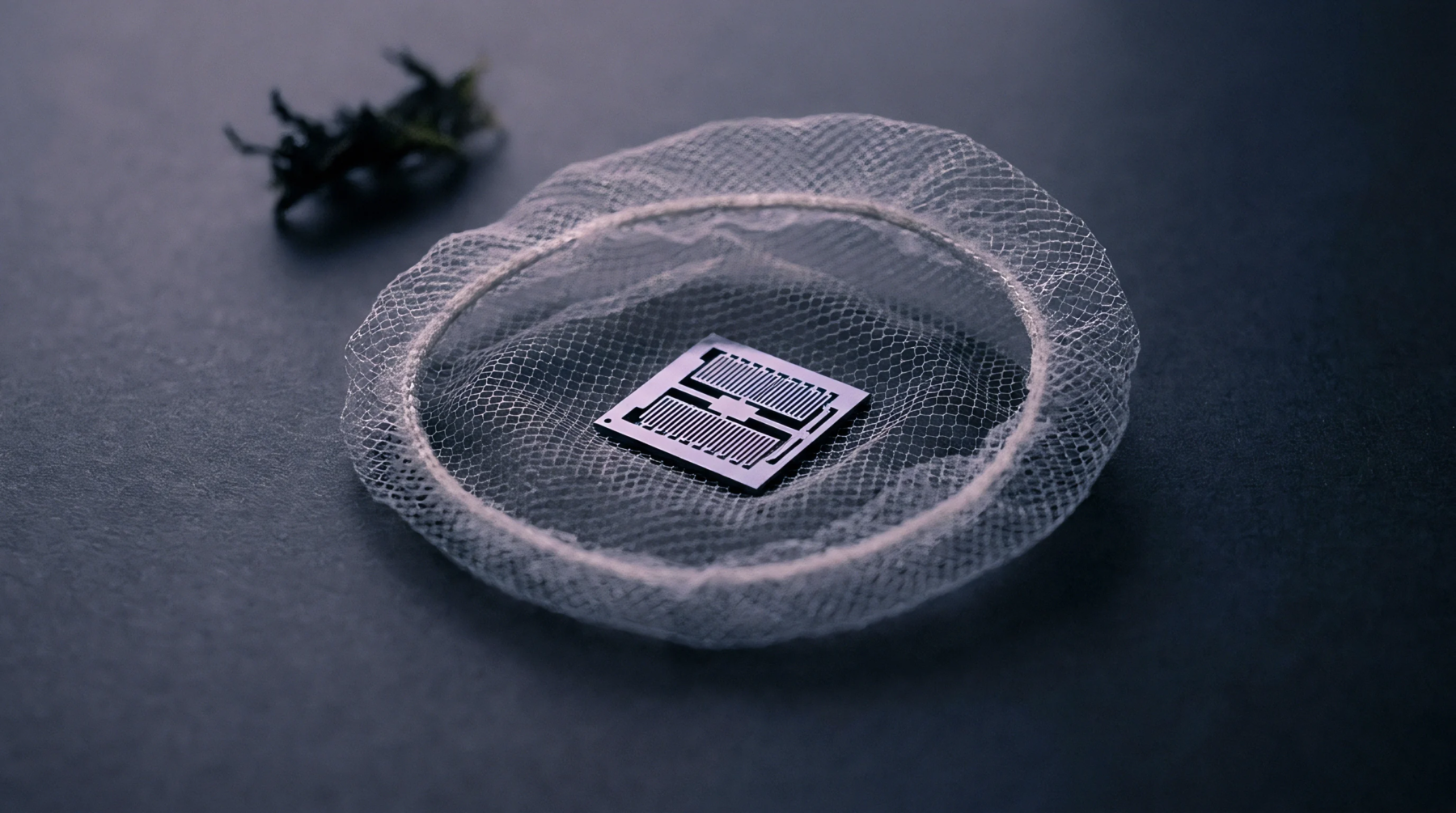
Reflow Popcorning Inspection Procedures and Acoustic Microscopy Delamination Criteria
Component reflow popcorning occurs when trapped moisture vaporizes during soldering; acoustic microscopy detects internal delamination via signal phase inversion.
Component reflow popcorning occurs when trapped moisture vaporizes during soldering; acoustic microscopy detects internal delamination via signal phase inversion.

Baking moisture sensitive ICs requires matching package thickness and carrier heat ratings to balance desorption speed against intermetallic lead oxidation risks.

Modelling hygrothermal stress requires superposing thermal strain, moisture swelling, and superheated steam pressure at leadframe interfaces during 260°C reflow.

High modulus mold compounds induce dynamic calibration shifts in sensors; sourcing specs must cap flexural modulus below 18 GPa to protect signal accuracy.

Fine-pitch iso-die variants exhibit divergent zero-point offset drift governed by package compliance, substrate CTE mismatch, and mechanical piezoresistive stress transfer.

Packaging thermal expansion mismatch generates die stress that converts to electrical offset drift via piezoresistive coupling and polymer viscoelastic creep.

Dual stage Langmuir kinetics dictate that bound moisture desorbs into steam during reflow, driving delamination and sensor offset drift unless bake profiles clear bound water.

Mitigate bandgap thermal stress errors using compliant leaded packages, PCB isolation slots, polyimide die buffers, and stabilized factory calibration.
Silicon die thermal expansion mismatches induce structural packaging stresses that warp inertial sensing combs, causing uncorrected thermal bias drift.

Polymer package modulus drops and thermal expansion jumps across glass transition destabilize MEMS gyroscope anchors, producing uncompensated zero rate bias.

Calculating desorption kinetics and activation energy via multi-ramp thermal testing determines safe reflow limits and prevents package popcorning.
Rigorous baseline and reference standard calibration across thermal analysis tools prevents erroneous resin approvals and down-line microelectronic assembly yield loss.

Extracting temperature-dependent interfacial fracture toughness along etched copper prevents reflow delamination and eliminates costly acoustic scan yield loss.

Silicon bandgap thermal drift inside microcontrollers creates parabolic ADC gain errors that package stress and reflow worsen, requiring careful compensation.
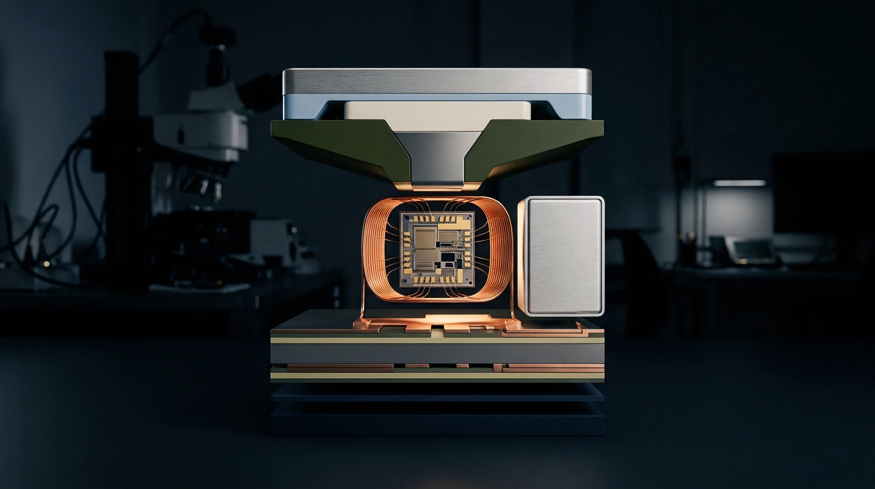
Procuring sensor mold compounds requires locking down glass transition, modulus, extractable halogens, and cold chain limits to prevent die stress and drift.

Post-assembly thermo-mechanical drift limits require tracking package CTE mismatch, solder standoff compliance, and viscoelastic mold relaxation across life.
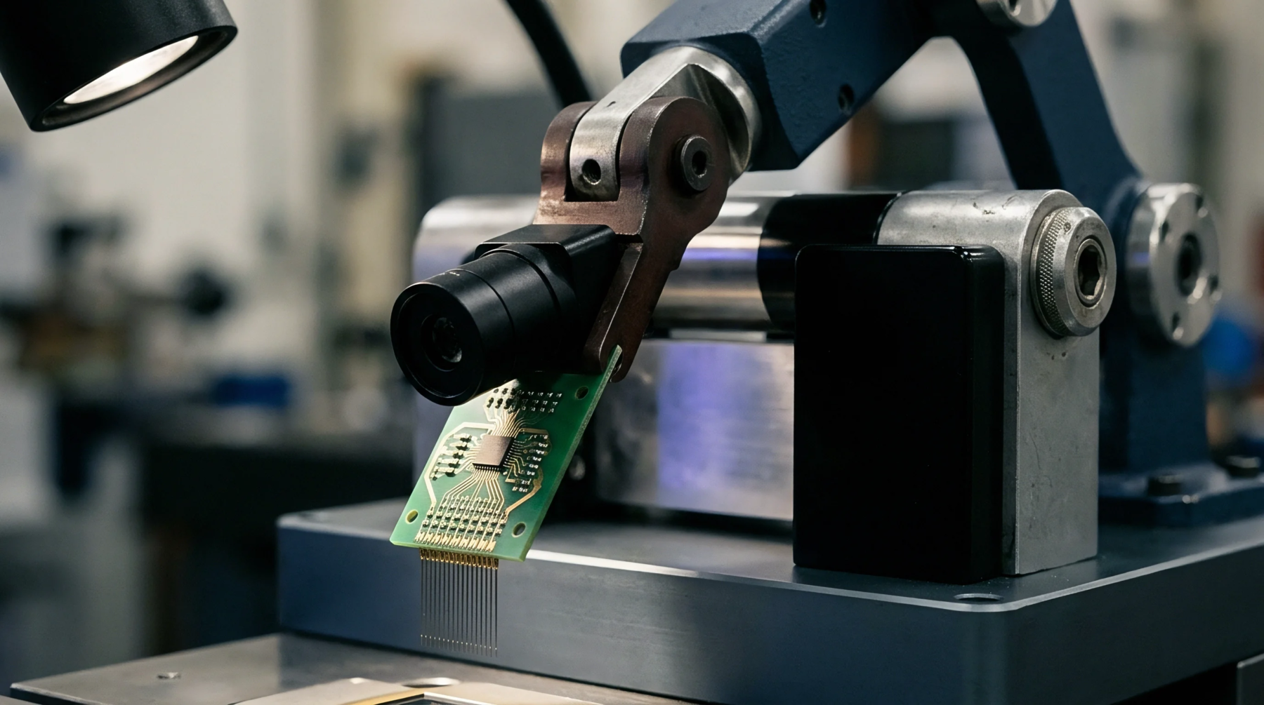
Characterize mold compound viscoelastic relaxation and decouple board strain through routing slots to prevent unrecoverable long-term sensor calibration drift.

Unpassivated wafer conversion packaging transfers mold compound reflow stresses directly into analog trim circuits, shifting factory register offsets.
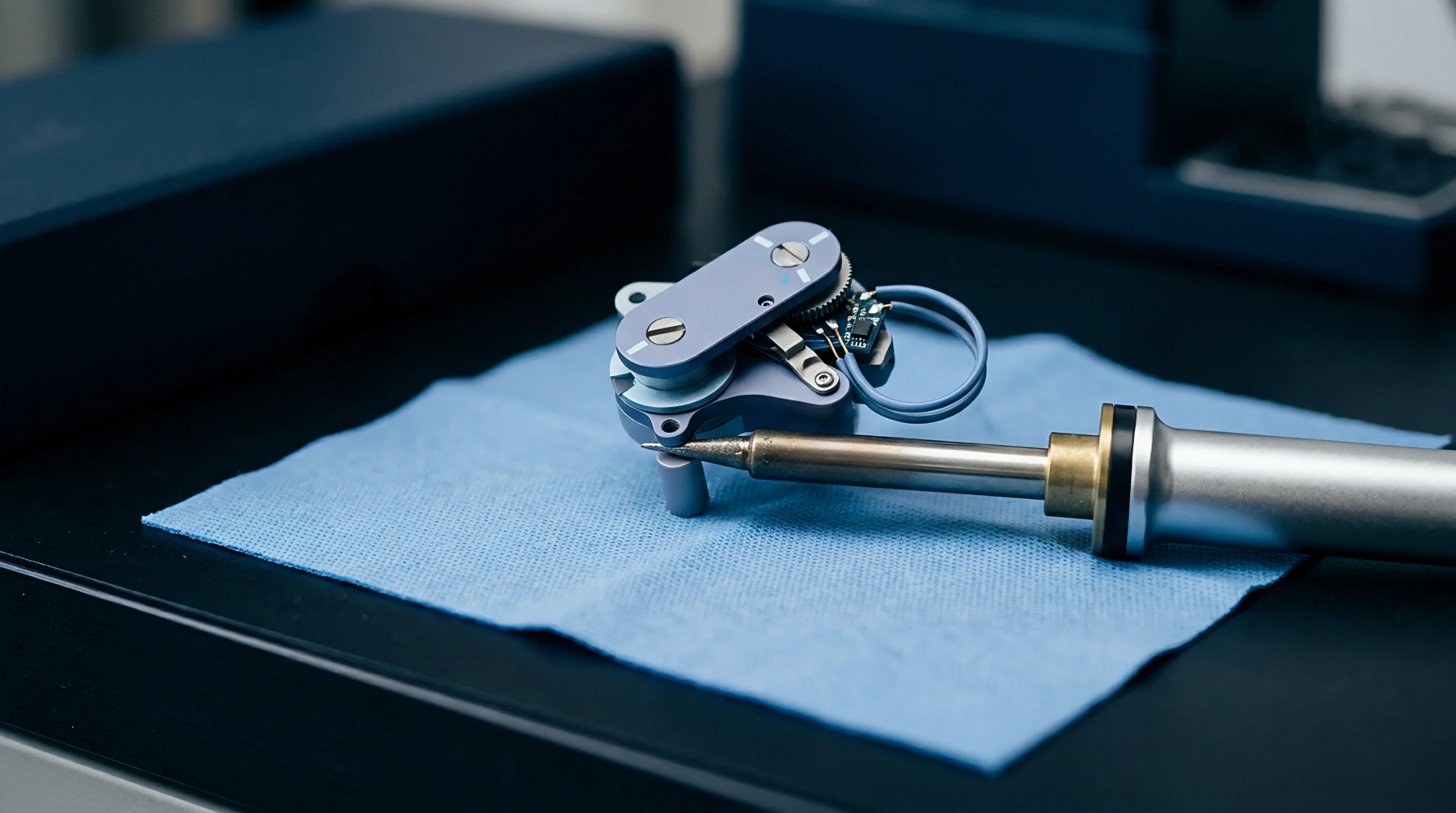
Thermal expansion mismatch in fine-pitch packages concentrates shear strain in outer joints, demanding matched underfill and strict standoff control to survive.

Post-reflow zero-point drift stems from package-to-board thermal expansion mismatch, demanding compliant leads or post-assembly firmware calibration.

Viscoelastic mold compound relaxation during thermal cycling alters sensor die stress, causing unrecoverable analog drift unless modeled via Prony series.

Lead-free reflow generates high interfacial shear stresses across LGA pads, driving piezoresistive offset shifts that demand post-bake calibration routines.

Encapsulant moisture saturation lowers matrix glass transition temperatures and generates destructive internal vapor pressures exceeding four megapascals at reflow.

Dual stage Carter Kibler diffusion modeling predicts bound moisture retention and prevents catastrophic package popcorning during high temperature surface reflow.

Plastic sub-bandgap references shift up to 300 ppm across thermal cycling due to mold compound viscoelastic creep, requiring mechanical keep-outs or ceramic forms.

Hygroscopic swelling in packaging polymers transfers parasitic shear into MEMS diaphragms, causing zero-point drift that demands pedestal isolation.
Post-package bandgap voltage reference drift stems from mold compound thermal strain and moisture swelling, requiring ceramic packaging or stress-isolated PCB layouts to maintain sub-10 ppm accuracy.

Surface mount packaging transfers printed circuit board flexure to piezoresistive silicon dies, causing bridge zero shifts that defeat digital compensation.
Calculate viscoelastic stress transfer by fitting multi-mode Prony series DMA data and applying Arrhenius-corrected shift factors under thermal cycling dwells.

Anisotropic silicon strain tensors corrupt precision converter references; selecting compliant leadframes or ceramic cavities prevents uncorrectable drift.
Expertise is a utility, not a secret. sentiention™ publishes its working knowledge as open reference: intelligence layer covering the materials it sources, the markets it enters, and the reference that serves both.