Silicon Die Thermal Expansion Mechanics in Micro Inertial Sensors
Silicon die thermal expansion mismatches induce structural packaging stresses that warp inertial sensing combs, causing uncorrected thermal bias drift.


Warp
Thermal expansion mismatches inside microelectromechanical inertial sensors convert ambient temperature shifts into mechanical strain across the micromachined proof mass suspension. Single-crystal silicon exhibits a coefficient of thermal expansion between 2.56 × 10⁻⁶ /K and 2.62 × 10⁻⁶ /K at room temperature. Copper leadframes, printed circuit laminates, and epoxy mold compounds present thermal expansion coefficients ranging from 12 × 10⁻⁶ /K to 17 × 10⁻⁶ /K. When the temperature shifts by 40 K, differential expansion between the structural die and the packaging substrate produces interfacial shear forces that travel through the die-attach adhesive.
These interfacial forces bend the silicon substrate, displacing stationary capacitive sense electrodes relative to suspended proof masses.
The resulting physical deflection alters nominal capacitance gaps measured in micrometers. A typical sub-millimeter inertial sensing cell features capacitive comb gaps between 1.0 µm and 2.5 µm. Out-of-plane warping of only 15 nanometers across a 2 mm die generates an asymmetric gap variation large enough to emulate an acceleration input of several tens of milli-g.
When packaging materials undergo repeated temperature swings from -40 °C to 125 °C, differential thermal contraction curves impose variable mechanical moments on the internal silicon anchors. The structural deformation shifts the resting zero-point of the sensor bridge before any external acceleration or angular rate acts upon the package.
Temperature gradients across symmetric die geometries create asymmetric differential capacitance independent of true applied acceleration.
Substrate warpage follows classical bi-material plate bending mechanics modified by the non-linear elasticity of organic die adhesives. Thick silicon substrates resist bending moments through higher area moments of inertia, yet thinning dies to 150 µm or 100 µm for compact multi-axis packages increases mechanical compliance. Thinned silicon yields to external packaging stresses readily, transferring board-level soldering deformation directly into the structural micromachined layer.
| Material | Expansion (ppm/K) | Modulus (GPa) | Conductivity (W/m·K) | Poisson Ratio |
|---|---|---|---|---|
| Single Crystal Silicon (100) | 2.59 | 130 | 148 | 0.28 |
| Single Crystal Silicon (110) | 2.59 | 169 | 148 | 0.06 |
| Borosilicate Glass (Pyrex 7740) | 3.25 | 63 | 1.1 | 0.20 |
| Alumina Ceramic (Al2O3 96%) | 6.70 | 300 | 24 | 0.22 |
| Copper Alloy Leadframe (C194) | 16.30 | 121 | 260 | 0.33 |
| FR4 Circuit Laminate (X-Y Plane) | 14.50 | 22 | 0.3 | 0.14 |
| Epoxy Mold Compound (Filled) | 10.50 | 25 | 0.9 | 0.25 |
Material selections determine the amplitude of package-induced bias shifts across temperature. Ceramic chip carriers match the silicon expansion curve closer than organic resin packages, lowering the total mechanical strain transferred to the sensing core. Die-attach selection introduces another variable, balancing elastic compliance against structural creep over operational lifespans.
- Interfacial Delamination occurs when cyclic thermal shear stress exceeds the adhesive shear strength at the die pad interface, creating localized stress concentrations that alter mechanical boundary conditions permanently.
- Capacitive Offset Drift manifests as steady baseline shifts when asymmetric die bending changes the differential comb overlap area across the suspension plane.
- Resonance Frequency Detuning develops when package stress compresses silicon spring beams, shifting the mechanical resonance point of drive and sense modes away from the phase-locked excitation loop.
- Solder Joint Fatigue introduces time-dependent tilt angles into surface-mounted inertial packages, corrupting multi-axis cross-axis sensitivity matrices during prolonged thermal cycling.
Neglecting die-level packaging expansion mechanics leads to permanent calibration offsets, uncorrectable thermal drift curves, and product recalls when vehicle stability modules or navigation systems encounter field temperature swings.


Anisotropy
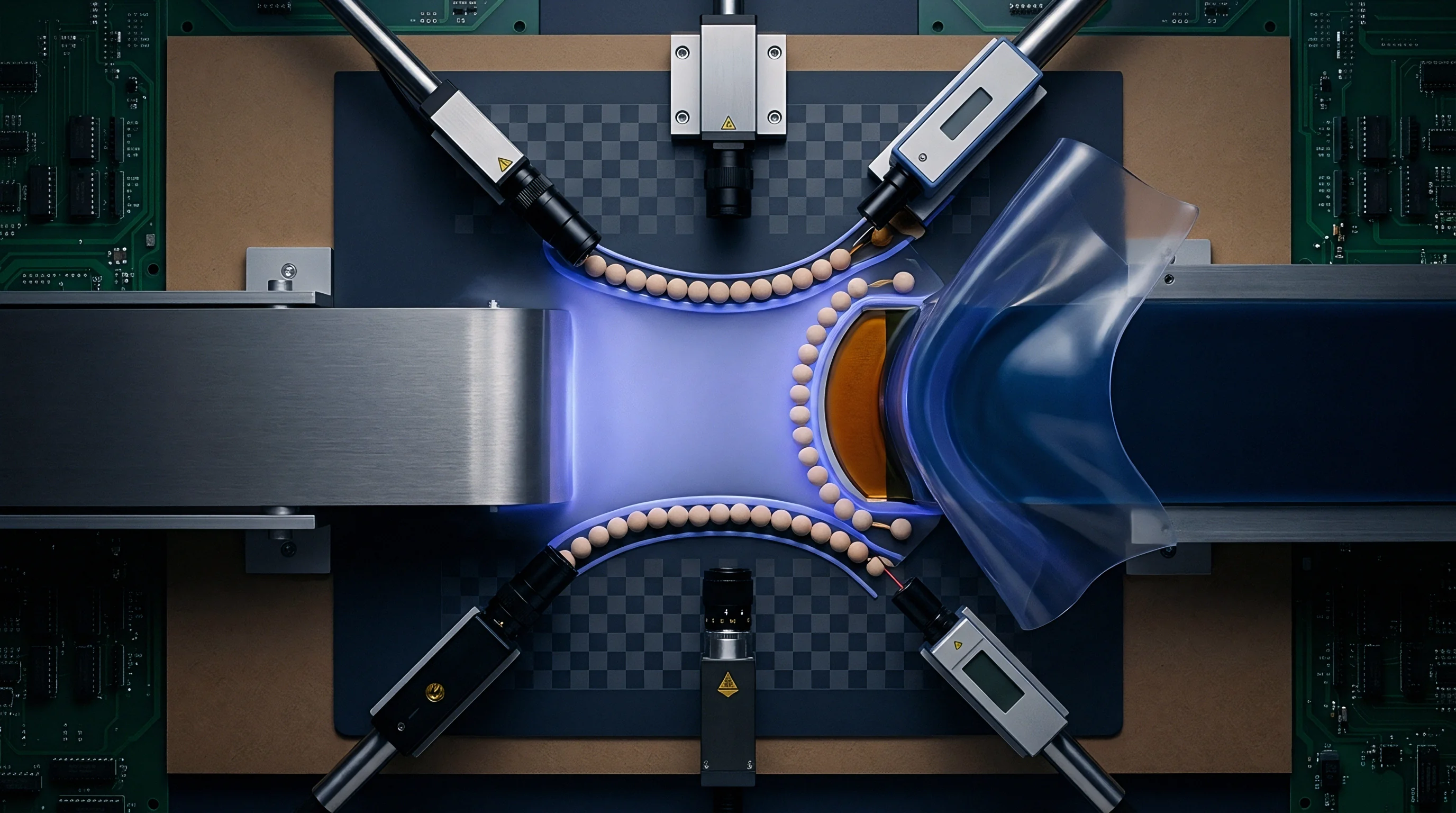
Crystalline structure dictates the direction-dependent elastic behavior of silicon under applied thermal stress. Silicon belongs to the cubic crystal class, which means its stiffness tensor contains three independent elastic constants: c11 equals 165.7 GPa, c12 equals 63.9 GPa, and c44 equals 79.6 GPa. Young’s modulus varies dramatically with orientation, dropping to 130 GPa along the <100> crystallographic direction and rising to 188 GPa along the <111> direction.
In the commonly used (100) wafer plane, Young’s modulus exhibits fourfold symmetry with a minimum along <100> axes and a maximum of 169 GPa along <110> axes.
Why Does Crystallographic Alignment Alter Bias Drift?
Suspension beams aligned along different wafer axes react with unequal stiffness when subjected to uniform packaging compression. If an accelerometer suspension utilizes orthogonal flexure beams oriented along the <110> and <100> directions, isotropic packaging expansion generates anisotropic restoring forces. The suspension experiences unequal spring constant shifts along orthogonal sensing axes, causing scale factor cross-axis sensitivity to drift with temperature.
Single-crystal silicon exhibits a temperature coefficient of Young modulus of -64 ppm/K along the <110> direction between -40 °C and 85 °C.
The temperature coefficient of elasticity creates an intrinsic thermal dependence in the mechanical spring rate. As temperature rises, interatomic bonds loosen and the silicon lattice softens. Because the mechanical resonance frequency scales with the square root of spring stiffness divided by mass, the natural frequency of an inertial resonator drops predictably as ambient temperature increases.
- Wafer Orientation Selection balances lithographic etching behavior against mechanical stiffness, with (100) wafers favoring anisotropic wet etching and (111) wafers providing isotropic in-plane elastic properties.
- Piezoresistive Coefficient Mapping dictates sensor layout angles to minimize parasitic stress sensitivity in capacitive dies or maximize signal response in piezoresistive strain gages.
- Comb Finger Alignment along principal stiffness axes limits out-of-plane curling during uniform temperature elevation.
- Thermal Expansion Matching requires aligning sensor axes with the principal thermal expansion axes of anisotropic composite package materials.
Fabrication houses often defend thermal scale factor errors by pointing out that standard silicon foundry runs maintain wafer crystal orientation tolerances within 0.5 degrees of nominal crystallographic planes.
Anchor
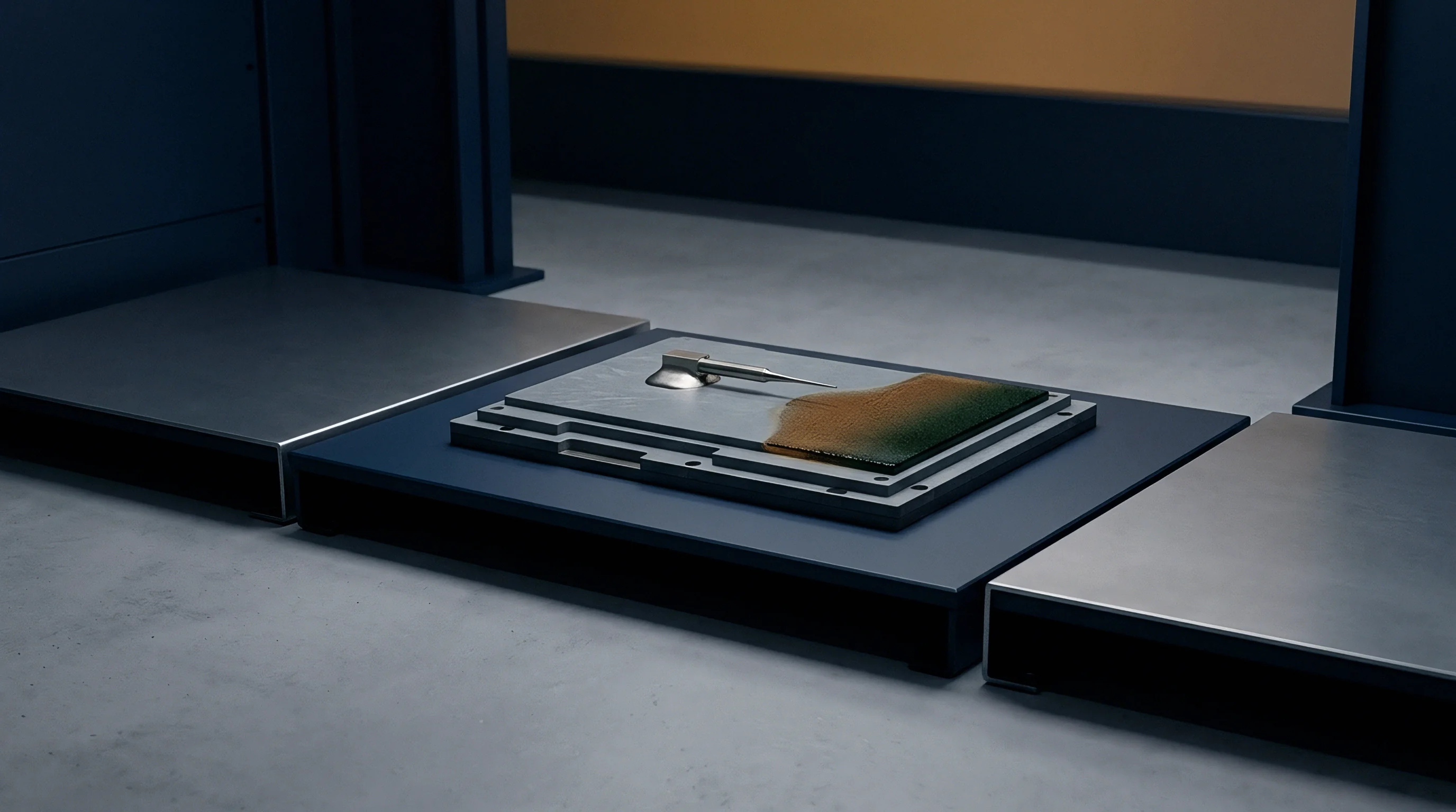
Mechanical anchoring points fix the micromachined silicon structure to the underlying support substrate. An anchor defines the kinematic boundary through which all package-induced thermal strains enter the delicate proof mass suspension. Multiple distributed anchors distribute stress directly into the spring beams.
When the underlying glass or silicon carrier expands faster than the active sensor layer, the physical distance between separate anchors expands proportionally. This displacement directly loads the internal suspension springs, inducing large shifts in sensor zero-g bias and resonant frequency.
Single central anchor designs mitigate this expansion transfer by allowing the surrounding silicon frame to expand freely outward from a single reference point. The frame expands according to its own expansion coefficient without fighting the substrate underneath.
Centralized single-point anchor topologies isolate proof mass suspensions from substrate strain fields.
| Anchor Topology | Stress Transfer (%) | Bias Shift (mg) | Quadrature Drift (°/s) | Drop Shock Survival (g) |
|---|---|---|---|---|
| Quad-Corner Anchors | 68.4 | 145 | 12.4 | 10000 |
| Dual Symmetrical Anchors | 31.2 | 52 | 4.1 | 7500 |
| Single Central Anchor | 4.6 | 6 | 0.5 | 3500 |
| Suspended Isolation Ring | 1.8 | 2 | 0.2 | 2000 |
A central anchor configuration decreases mechanical survivability under extreme shock loads. A trade-off governs anchor topology selection between environmental thermal stability and mechanical shock robustness.
- Substrate Cavity Etching creates a recess beneath the active mechanical structure to prevent out-of-plane contact during thermal expansion.
- Anchor Post Deposition establishes rigid bonding locations on the substrate while preserving clearance for surrounding kinematic stress-relief rings.
- Compliant Spring Routing routes serpentine stress-decoupling beams between the anchor post and the rigid outer suspension frame.
- Differential Sense Finger Placement positions capacitive combs symmetrically around the anchor to cancel common-mode thermal dilation algebraically.
Sensing engineers continue to debate whether nested decoupling rings can provide automotive-grade shock resistance without introducing parasitic low-frequency vibration modes into the sensing bandwidth.


Hysteresis
Inelastic material phenomena inside the die stack convert transient thermal excursions into permanent or semi-permanent sensor output offsets. While single-crystal silicon remains perfectly elastic below 500 °C, the surrounding packaging materials behave viscoelastically. Die-attach adhesives, underfill resins, and epoxy mold compounds undergo relaxation when held at elevated temperatures.
When an inertial sensor heats to 85 °C during operation, the adhesive softens and relieves built-in packaging stress through polymer chain rearrangement.
Upon cooling back to room temperature, the polymer chains cannot instantly return to their initial configuration. The resulting stress state differs from the initial state, producing thermal hysteresis in the zero-rate output of gyroscopes and the zero-g offset of accelerometers. This shift persists until the material reaches mechanical equilibrium.

When Does Polymer Creep Defeat Factory Calibration?
Polymer relaxation rates depend heavily on the operating temperature relative to the glass transition temperature of the die attach material. When the operating environment crosses the glass transition point, the elastic modulus of the adhesive drops by two orders of magnitude, accelerating creep rates. Subsequent cooling locks in residual shear stresses across the silicon anchor pads.
Factory calibration algorithms that assume static, single-valued temperature-to-offset curves fail to track these path-dependent stress states.
AEC-Q100 Grade 1 thermal cycling between -40 °C and 125 °C exposes path-dependent bias hysteresis in high-modulus epoxy die attach systems.
Metallic eutectic bonding materials, such as gold-tin or gold-silicon alloys, eliminate polymer creep entirely. Eutectic bonds introduce higher baseline residual stresses during initial solid-state cooling due to high processing temperatures. Hard metallic joints transmit printed circuit board flexure into the die without attenuation.
Compliant silicone die adhesives dampen external mechanical strain effectively while introducing long-term moisture absorption risks that distort the package over operational lifespans.

Arithmetic
Compensating for thermomechanical bias drift requires mathematical polynomial modeling inside on-chip signal processors. A typical digital inertial sensor integrates an internal bandgap temperature sensor alongside the mechanical sensing core. The conditioning circuitry reads the local temperature and applies a polynomial correction to the raw digital output register.
The compensated output represents a function of temperature according to the following algebraic formulation.
Let T denote the instantaneous measured temperature and T0 represent the calibration reference temperature. The uncompensated acceleration output a_raw experiences offset drift described by a polynomial series:
a_comp = a_raw – (c0 + c1·(T – T0) + c2·(T – T0)² + c3·(T – T0)³)
The polynomial coefficients c0 through c3 are computed during factory multi-temperature screening and burned into on-die non-volatile registers. Higher-order polynomials capture non-linear substrate bending mechanics more accurately across wide thermal ranges.
| Fitting Model | Residual Bias (mg) | Angle Random Walk Impact | Calibration Points | Factory Test Time (s) |
|---|---|---|---|---|
| Linear (1st Order) | 18.4 | None | 2 | 45 |
| Quadratic (2nd Order) | 4.2 | Negligible | 3 | 120 |
| Cubic (3rd Order) | 0.8 | +5% Register Overhead | 4 | 210 |
| 4th Order with Rate | 0.3 | +12% Processing Power | 5 | 360 |
Fast thermal transients create dynamic thermal gradients across the die that static temperature polynomials cannot correct. If the internal thermometer sits 1.5 mm away from the mechanical sensing combs, a rapid ambient thermal ramp creates an internal temperature lag. The thermometer reports a temperature corresponding to a stress state that has already evolved or not yet arrived at the proof mass suspension.
Advanced sensor architectures incorporate dual temperature sensors or rate-of-change derivative terms into the compensation engine to correct for dynamic thermal lag errors. Calibration factory time scales directly with the number of thermal setpoints, dictating the ultimate bill-of-materials cost of tactical-grade micro-inertial components.
Under procurement contracts referencing IEEE 1293 standards for inertial sensor testing, suppliers must guarantee residual bias stability limits across specified temperature ramp rates rather than static thermal soak conditions alone.