Sourcing Specifications for High Modulus Package Mold Compounds Causing Dynamic Calibration Shift Limits
High modulus mold compounds induce dynamic calibration shifts in sensors; sourcing specs must cap flexural modulus below 18 GPa to protect signal accuracy.


Resin
Post-mold shrinkage and thermal expansion mismatches allow packaging polymers to exert substantial mechanical force directly onto encapsulated silicon dies. When epoxy formulations use silica filler loadings above 85 percent by weight to keep moisture absorption down, they surround delicate micro-electro-mechanical structures with an unyielding matrix. That rigidity channels ambient thermal swings and PCB flexure straight into the die’s active area, warping capacitive sensing gaps and piezoresistive bridges.
Whenever the room-temperature flexural rigidity of the encapsulation exceeds 20 GigaPascals, precision sensor ICs show marked zero-point drift and span sensitivity errors.
Surface mount reflow pushes package temperatures past the compound’s glass transition point, temporarily wiping out internal residual stresses before locking in a high-stress equilibrium on cooldown. The polymer matrix then spends hundreds of hours relaxing at room temperature. This slow relaxation produces a subtle calibration creep that standard, short-window factory tests never catch.
Specifying rigid encapsulants without planning for long-term strain relaxation routinely leads to field failures once sensor outputs drift outside their target specification windows.
Silica filler concentrations above 88 weight percent reduce moisture absorption below 0.15 percent while increasing room temperature flexural modulus past 24 GigaPascals.
Soft organic coatings and silicone gel buffers over the active die surface absorb some incoming strain, but lateral shear carried through corner leads still creates uneven stress fields across the chip. These localized gradients cause anisotropic piezoresistive shifts that host microcontrollers cannot fix with simple isotropic temperature polynomials. The drift shows up as a non-repeatable offset whenever the package undergoes thermal ramps exceeding 2 degrees Celsius per minute.

Mechanical Strain Coupling Mechanisms
Stress transfer from package to die depends heavily on the interfacial shear strength between the mold compound and the silicon nitride passivation. High-modulus formulations generate shear adhesion values over 15 MegaPascals, locking the interfaces together without mechanical slip. Without slip, differential thermal contraction translates directly into mechanical loading across the underlying circuitry.
- Anisotropic Stress Gradients Asymmetric mold flow during transfer molding aligns filler particles directionally, yielding orthogonal elastic modulus variations of more than 15 percent across the die plane.
- Post-Cure Polymer Shrinkage Cross-linking during post-mold cure causes a 0.10 to 0.25 percent volumetric contraction, permanently loading embedded sensor elements in compression.
- Differential Expansion Mismatch Below the glass transition temperature, compound expansion coefficients span 8 to 12 parts per million per Kelvin, compared with just 2.6 parts per million per Kelvin for pure silicon.
- Hysteresis in Glass Transition Non-linear modulus decay through the glass transition zone prevents sensor output circuits from returning to their initial baseline voltages after seeing elevated temperatures.
Using stiff encapsulants without flexible die-attach adhesives shunts mechanical loads to the die perimeters, inviting micro-cracking and step-changes in calibration baseline after thermal shock.

Modulus
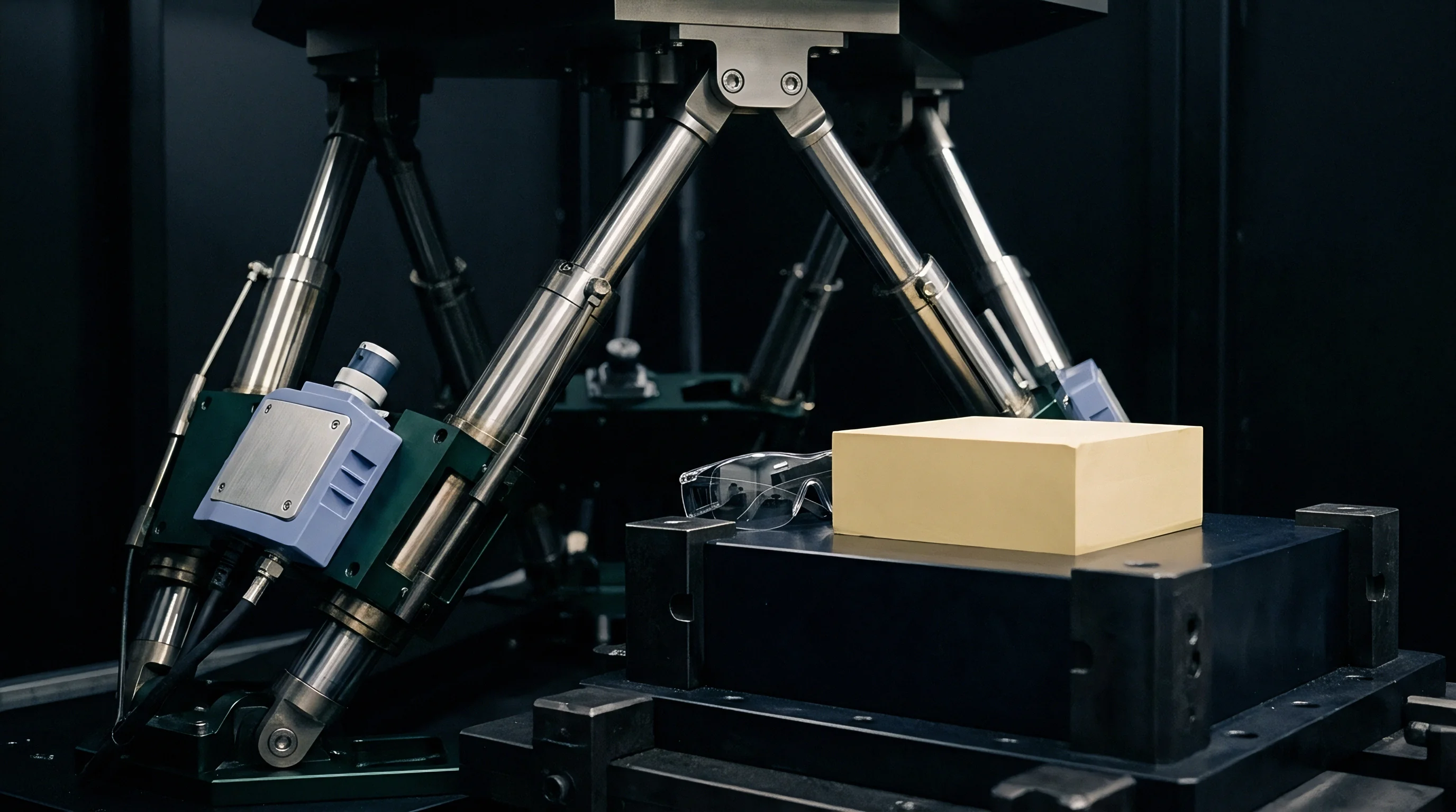
Polymer matrix stiffness specifications require tight numerical limits across the entire operating temperature range. Flexural rigidity drops sharply at the glass transition point, collapsing from tens of GigaPascals to single-digit values and fundamentally altering assembly stress. Standardized thermomechanical testing, via ASTM E831 or ISO 11359-2, outlines the exact storage modulus profile needed to qualify incoming compound.
Procurement documentation must specify boundaries for both the glassy modulus at low temperatures and the rubbery modulus at high temperatures to prevent uncontrolled strain shifts in the field.
Epoxies formulated for low moisture uptake pair dense aromatic resins with high spherical silica loadings. The combination blocks humidity-driven swelling, but the added stiffness couples mechanical strain straight into the die. Thermogravimetric and dynamic mechanical analysis show that exceeding a 22 GigaPascals flexural modulus at 25 degrees Celsius triples thermal hysteresis offsets compared to compliant 14 GigaPascals materials.
Standard qualification protocols relying solely on room temperature mechanical testing fail to reveal high-temperature rubbery modulus variations that cause dynamic calibration shift limits to be exceeded.
Suppliers sometimes modify filler particle distributions between lots to hit melt viscosity targets without noting the change on datasheets. These unannounced adjustments move the filler network’s percolation threshold, shifting the composite storage modulus and altering the creep profile of the final component. Sourcing contracts need to enforce lot-by-lot physical property testing before compound is cleared for molding.

Material Specification Parameters and Stress Impact
Preventing dynamic calibration drift requires firm guardrails on core thermomechanical properties. Published datasheet numbers are typically batch averages that conceal wide lot-to-lot spread unless bounded by explicit quality provisions.
| Parameter | Measurement Standard | Target Range | Shift Risk Impact |
|---|---|---|---|
| Flexural Modulus (25°C) | DMA (ASTM E1356) | 12 to 18 GPa | Values above 20 GPa double piezoresistive drift rates |
| Glass Transition (Tg) | TMA (ISO 11359-2) | 150°C to 175°C | Low Tg causes unexpected modulus drops during reflow |
| CTE 1 (Below Tg) | TMA (ASTM E831) | 8 to 11 ppm/°C | Mismatch with silicon (2.6 ppm/°C) drives steady-state strain |
| CTE 2 (Above Tg) | TMA (ASTM E831) | 32 to 42 ppm/°C | High CTE 2 creates severe residual stress during cooling |
| Moisture Absorption | J-STD-020 (85°C/85%RH) | Below 0.12% | Hygroscopic expansion alters zero-point calibration |
Procurement teams must review compound behavior across every operating parameter at once rather than optimizing single metrics. Balancing moisture resistance against structural stiffness remains the primary challenge when defining packaging specs for precision devices.

Material Verification and Quality Control
Incoming inspection has to catch out-of-spec raw material before lots reach the transfer molding presses. Screening chemical properties via differential scanning calorimetry flags incomplete resin cross-linking before packaging high-value silicon.
- Storage Modulus Verification Dynamic mechanical analysis testing verifies that storage modulus values remain within a plus or minus 5 percent window across the entire specified temperature range.
- Filler Distribution Audit Laser diffraction particle size analysis confirms that spherical silica distributions adhere to the maximum packing density profile specified in the engineering drawing.
- Outgassing and Weight Loss Thermogravimetric analysis limits volatile organic content loss to less than 0.05 percent by weight during post-mold cure processing at 175 degrees Celsius.
- Viscosity Matrix Tracking Slit-die rheometry verifies that compound melt viscosity during mold filling stays within specified Pascal-second bounds to prevent wire sweep and die tilt.
Post-thermal property shifts are frequently characterized as benign secondary polymer curing, though they can equally indicate non-conforming raw compound.


Hysteresis
Thermal cycling sets up alternating stress fields inside encapsulated packages, resulting in non-linear sensor output curves. When temperatures shift rapidly, a lag develops between surface thermal changes and the dissipation of internal stress, manifesting as dynamic response drift. Conditioning circuitry tries to linearize output using digital correction algorithms, but mechanical hysteresis breaks the expected relationship between measured package temperature and actual die strain.
High-precision analog paths pick up uncorrectable errors as a result.
Small-outline IC packages housing piezoresistive pressure sensors display significant zero-point drift under thermal cycling from -40 degrees Celsius to +125 degrees Celsius. Viscoelastic relaxation releases elastic strain stored in the stiff mold compound very slowly, shifting zero-pressure differential readings by several millivolts over hours. Conventional linear temperature compensation cannot follow this kind of time-dependent drift, leaving host systems with uncalibrated offsets.
Mechanical stress relaxation within high modulus mold materials converts deterministic thermal expansion into time-dependent calibration uncertainty.
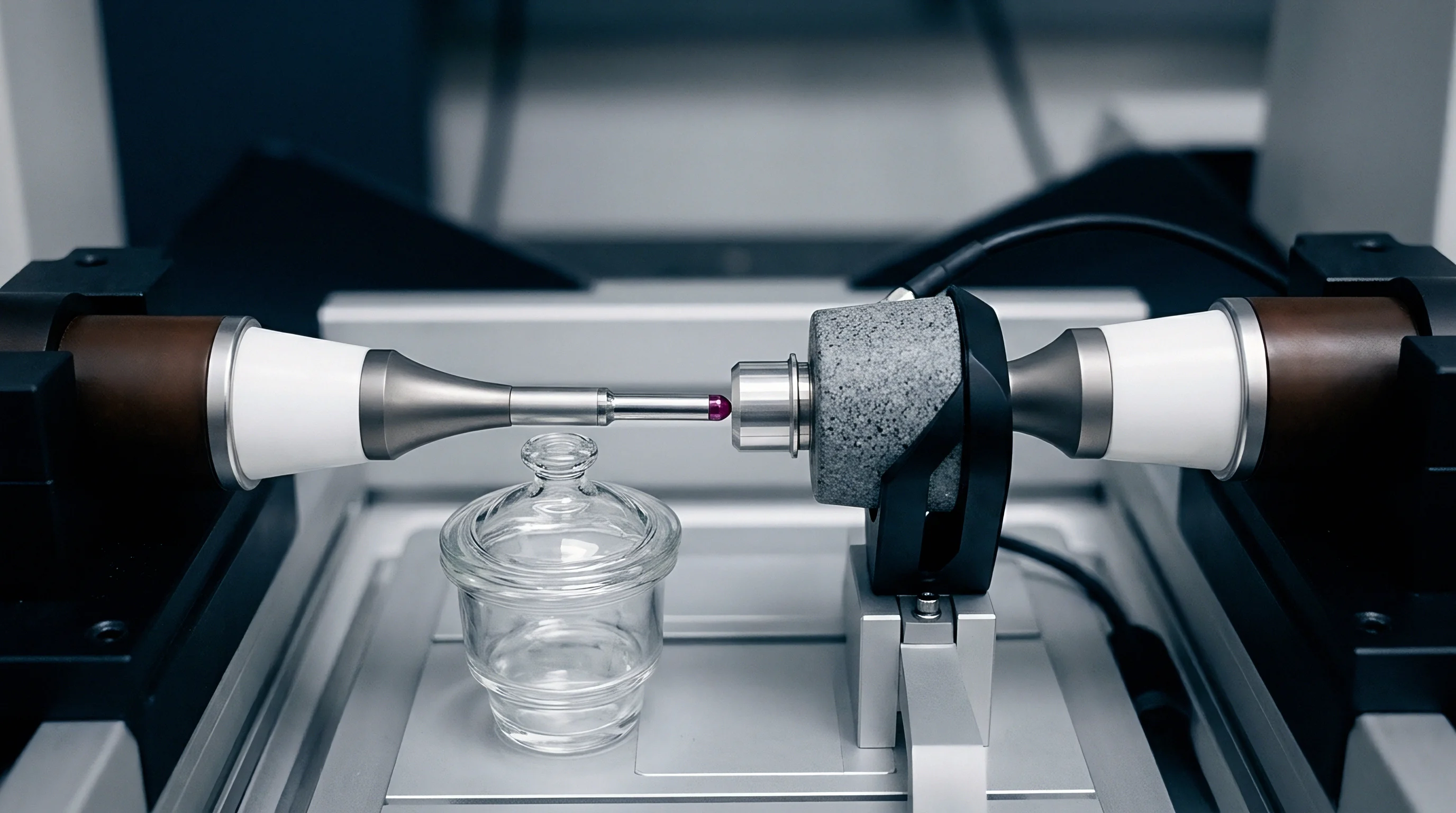
Separating transient thermal loads from permanent structural deformation requires real-time strain acquisition during environmental qualification. Piezoresistive strain rosette test dies confirm that high-modulus compounds can transfer up to 80 percent of board-level bending directly into active die circuitry. Lowering the compound modulus reduces this mechanical coupling and stabilizes baseline electrical readings.
Where Does Thermo-Mechanical Drift Bypass Firmware Calibration?
Firmware lookup tables rely on a single-valued relationship between ambient temperature and sensor offset. Thermomechanical hysteresis breaks that model: the sensor outputs two distinct values at the exact same temperature, dictated by whether the device arrived from a hotter or colder state. Static polynomial routines cannot correct this spread.
Looking at mechanical stress in a bridge sensor makes the mathematical failure of static calibration obvious. Consider a piezoresistive wheatstone bridge with a longitudinal piezoresistive coefficient πL = 6.5 × 10⁻¹⁰ Pa-1. An unmitigated package stress variation Δ σ = 15 MPa induced by mold compound shrinkage alters the differential bridge output according to the relationship:
fracΔ VoutVin = πL · Δ σ
Substituting the stress and piezoresistive values into the expression yields:
fracΔ VoutVin = (6.5 × 10⁻¹⁰ Pa-1) × (15 × 106 Pa) = 9.75 × 10⁻³ V/V
That shift creates a 0.975 percent full-scale calibration error. On a 16-bit analog-to-digital converter with a 3.3-Volt full-scale span, the mechanical stress alone burns through more than 638 least significant bits, wiping out the system’s entire accuracy allocation.
| Compound Type | Modulus (GPa) | Thermal Hysteresis (%FS) | Recovery Time (Hours) | Max Drift Rate (ppm/°C) |
|---|---|---|---|---|
| High Modulus Standard Epoxy | 24.5 | 0.85 | 14.0 | 120 |
| Ultra-Low Stress Epoxy | 14.2 | 0.18 | 1.5 | 25 |
| Silicone Gel Encapsulated Hybrid | 3.5 | 0.04 | 0.1 | 5 |
| Flexible Anisotropic Matrix | 11.0 | 0.12 | 0.8 | 18 |
Attempting to smooth this dynamic creep in software requires long filter time constants, which drastically cuts sensor bandwidth and sluggishly degrades dynamic response.

Diagnostic Sequence for Dynamic Offset Detection
Distinguishing silicon-level electrical failure from package-induced mechanical strain requires a structured bench procedure.
- Establish Room Temperature Baseline Record initial zero-input differential sensor output voltage at 25 degrees Celsius inside an environmentally controlled chamber after a 24-hour stabilization period.
- Execute Rapid Thermal Ramp Heat the environmental chamber to 125 degrees Celsius at a ramp rate of 10 degrees Celsius per minute while continuously logging sensor output data and internal temperature diode voltages.
- Isothermal Soak Phase Maintain the chamber at 125 degrees Celsius for 4 hours to record isothermal viscoelastic strain relaxation and output settling profiles.
- Cooling Cycle Execution Cool the chamber back to 25 degrees Celsius at 10 degrees Celsius per minute, monitoring for hysteresis loop area formation during the thermal transition.
- Post-Thermal Drift Analysis Compare final 25 degree Celsius output values against initial baseline data to quantify permanent thermomechanical calibration shift limits.
It remains unsettled whether long-term mechanical creep eventually plateaus after thousands of thermal cycles or continues to erode sensor calibration throughout the device’s working life.


Anchor
Board-level isolation prevents assembly strains from reaching the high-modulus package body. Solder land geometry, stencil opening dimensions, and routed PCB slots act as mechanical isolators that damp out flexure before it travels into the leads. Placing ground anchors and stress reliefs deliberately limits the shear forces reaching the molding compound when the board twists.
Quad-flat no-lead (QFN) footprints soldered to thick copper planes face heavy mechanical constraints. The thermal expansion delta between FR4 boards (CTE near 16 ppm/°C) and the QFN body drives substantial strain into the encapsulant. Routing perimeter expansion slots around the footprint reduces transferred board strain by more than 65 percent, keeping baseline calibration stable over harsh thermal cycling.
Corner solder pads on leadless sensor packages transmit up to three times more mechanical strain to the die than center thermal ground pads.
Die-attach materials serve as internal mechanical buffers within the package cavity. Soft elastomeric fluorosilicones and silicone adhesives yield under lateral shear from the mold compound, shielding the sensitive silicon face. High-modulus conductive epoxies offer low electrical resistance for grounding, but they transmit that shear directly and compromise dynamic offset stability.

Substrate Isolation Implementation Procedure
1. Identify primary mechanical strain axes across the printed circuit board assembly using finite element flexure analysis.
2. Route mechanical strain relief slots completely through the PCB substrate parallel to the long axis of the sensor package body.
3. Apply asymmetrical land pattern designs that reduce solder fillet volume on package corners while maintaining mechanical retention on center leads.
4. Specify non-solder mask defined (NSMD) pads for all signal terminals to ensure uniform solder wetting and symmetrical joint compliance.
5. Restrict copper trace entry widths to less than 50 percent of the land pad width to prevent localized thermal mass imbalances during reflow solidification.
6. Verify final assembly strain levels using surface-mounted rosette strain gauges placed adjacent to the sensor package body during structural board deflection testing.

Assembly Level Stress Mitigation Failure Modes
Incorrectly implemented board-level strain reliefs introduce reliability hazards elsewhere in the assembly.
- Solder Joint Fatigue Failure Excessive solder pad flexibility increases mechanical strain on corner leads, accelerating fatigue solder cracking under continuous vibration environments.
- Asymmetric Solder Bridging Non-uniform stencil printing over stress-relief footprint designs leads to uneven solder joint height, inducing severe die tilt and baseline offset shifts.
- Substrate Delamination Risks Milling mechanical relief slots too close to internal copper power planes exposes glass fibers to moisture ingress, driving catastrophic conductive anodic filament growth.
- Underfill Void Formation Incomplete capillary flow of liquid underfills around dense pad arrays traps micro-air bubbles that expand during reflow, inducing localized stress concentrations on the die bottom surface.
Trimming the copper area directly under leadless packages softens the mechanical link between board laminate and package compound.


Contract
Procurement specifications for high-modulus mold compounds must include firm thermomechanical windows and dynamic calibration yield targets. Standard catalog datasheets show typical values that offer no contractual recourse when formulations drift between batches. Defining clear parameter boundaries tied to standard test methods holds compound vendors liable when dynamic calibration drift cuts into production yields.
Incorporate strict material acceptance criteria directly into raw material purchase agreements. Require suppliers to provide certified lot delivery dossiers containing dynamic mechanical analysis curves, thermogravimetric outgassing data, and laser diffraction particle size distributions for every shipped batch. Formulations exceeding specified flexural modulus or glass transition temperature boundaries must trigger automated inventory holds and financial chargebacks for affected production lots.

Commercial Variant Cost Vs Dynamic Shift Yield Floor
Choosing a package architecture involves direct trade-offs between raw material expense, packaging line yield, and long-term calibration limits. Standard high-modulus epoxies remain common because raw material costs are low and cure times are short, but downstream test fallout on precision sensor lines routinely wipes out those savings.
| Package Configuration | Encapsulant Compound Class | Relative Unit Cost | Yield Floor (% Calibration Pass) | Lot Rejection Risk |
|---|---|---|---|---|
| Standard QFN-24 | High Modulus Standard Silica | 1.00x | 91.2% | High |
| Exposed Pad LGA-16 | Low Modulus Ultra-Low Stress | 1.35x | 98.6% | Low |
| Cavity Gel-Filled LGA | Silicone Gel / Liquid Encapsulant | 2.10x | 99.7% | Very Low |
| Premolded SOIC-16 | Thermally Matched Elastomer | 1.75x | 97.4% | Medium |
The piece-part savings realized on cheap, rigid compounds quickly disappear once finished sensor assemblies begin failing dynamic calibration screens at volume.

Sourcing Contract Terms and Liability Clauses
Sound supply agreements rely on crisp definitions of material non-conformance, unambiguous test protocols, and defined financial remedies. Contract language must connect chemical property variances directly to downstream assembly yield fallout.
A comprehensive material procurement agreement incorporates a mandatory batch qualification clause. The clause specifies: Section 4.2 Material Consistency Standard – Supplier shall deliver Epoxy Mold Compound lots complying with Flexural Storage Modulus boundaries of 14.0 GPa to 17.5 GPa measured at 25 degrees Celsius per ASTM E1356. Any delivered lot exhibiting a storage modulus deviation exceeding plus or minus 5.0 percent from the qualified baseline sample shall be rejected at Supplier expense, including all transportation, testing, and production line downtime fees incurred by Purchaser.
A secondary clause addresses post-reflow dynamic stability guarantees: Section 8.5 Dynamic Calibration Shift Warranty – Encapsulation compound shall demonstrate thermomechanical stability such that 98.5 percent of finished sensor IC assemblies pass post-reflow dynamic offset calibration testing within plus or minus 0.25 percent full-scale limits. Should Purchaser experience calibration failure rates exceeding 1.5 percent attributable to compound physical property variation, Supplier shall reimburse Purchaser for the full landed cost of rejected active silicon assemblies.